- 您现在的位置:买卖IC网 > PDF目录1894 > AD9895KBCZRL (Analog Devices Inc)IC CCD SIGNAL PROC/GEN 64-CSPBGA PDF资料下载
参数资料
| 型号: | AD9895KBCZRL |
| 厂商: | Analog Devices Inc |
| 文件页数: | 35/58页 |
| 文件大小: | 0K |
| 描述: | IC CCD SIGNAL PROC/GEN 64-CSPBGA |
| 标准包装: | 2,000 |
| 类型: | CCD 信号处理器,12 位 |
| 输入类型: | 逻辑 |
| 输出类型: | 逻辑 |
| 接口: | 3 线串口 |
| 安装类型: | 表面贴装 |
| 封装/外壳: | 64-VFBGA,CSPBGA |
| 供应商设备封装: | 64-CSPBGA(9x9) |
| 包装: | 带卷 (TR) |
第1页第2页第3页第4页第5页第6页第7页第8页第9页第10页第11页第12页第13页第14页第15页第16页第17页第18页第19页第20页第21页第22页第23页第24页第25页第26页第27页第28页第29页第30页第31页第32页第33页第34页当前第35页第36页第37页第38页第39页第40页第41页第42页第43页第44页第45页第46页第47页第48页第49页第50页第51页第52页第53页第54页第55页第56页第57页第58页
REV. A
–40–
AD9891/AD9895
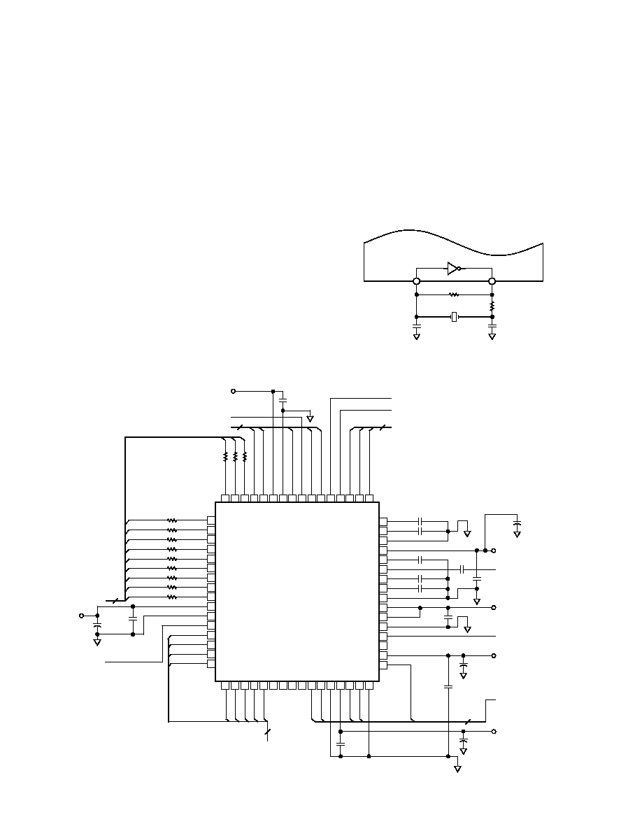
CIRCUIT LAYOUT INFORMATION
The AD9891/AD9895 Typical Circuit Connection is shown in
Figure 50. Note that Pins E1 and E2 will be No Connects when
using the AD9891. The PCB layout is critical in achieving good
image quality from the AD989x products. All of the supply pins,
particularly the AVDD1, TCVDD, RGVDD, and HVDD sup-
plies, must be decoupled to ground with good quality high
frequency chip capacitors. The decoupling capacitors should be
located as close as possible to the supply pins and should have
a very low impedance path to a continuous ground plane.
There should also be a 4.7
F or larger value bypass capacitor
for each main supply—AVDD, RGVDD, HVDD, and DRVDD
—although this is not necessary for each individual pin. In most
applications, it is easier to share the supply for RGVDD and
HVDD, which may be done as long as the individual supply
pins are separately bypassed. A separate 3 V supply may also be
used for DRVDD, but this supply pin should still be decoupled
to the same ground plane as the rest of the chip. A separate
ground for DRVSS is not recommended.
The analog bypass pins (BYP1–3, VRB, VRT) should also be
carefully decoupled to ground as close as possible to their re-
spective pins. The analog input (CCDIN) capacitor should also
be located close to the pin.
The H1–H4 and RG traces should be designed to have low
inductance to avoid excessive distortion of the signals. Heavier
traces are recommended because of the large transient current
demand on H1–H4 by the CCD. If possible, physically locating
the AD9891/AD9895 closer to the CCD will reduce the induc-
tance on these lines. As always, the routing path should be as
direct as possible from the AD9891/AD9895 to the CCD.
The AD9891/AD9895 also contains an on-chip oscillator for
driving an external crystal. Figure 51 shows an example appli-
cation using a typical 18 MHz crystal. For the exact values of
the external resistors and capacitors, it is best to consult with
the crystal manufacturer’s data sheet.
20pF
C10
20pF
500
1M
CLI
CLO
AD9891/AD9895
18MHz
XTAL
Figure 51. Crystal Driver Application
D0(LSB)
D2
D1
HD
DVDD
DVSS
VD
SYNC
CLPOB/PBLK
LD/FD
STROBE
MSHUT
SCK
SDI
SL
DCLK
V4
VSG1/V5
VSG2/V6
VSG3/V7
VSG4/V8
VSG5
VSG6
VSG7
VSG8
H1
H2
HVSS
TOP VIEW
(Not to Scale)
AD9895
REFT
REFB
AVSS2
AVDD2
BYP3
CCDIN
BYP2
BYP1
AVSS1
AVDD1
TCVDD
TCVSS
D3
D4
D5
D6
D7
D8
D9
D10
(MSB) D11
DRVDD
DRVSS
VSUB
3V
ANALOG
SUPPLY
OUTPUT FROM CCD
10
DATA OUTPUTS
SUBCK
V1
V2
V3
LINE/FIELD/CLAMP SYNC TO ASIC/DSP
3V
ANALOG
SUPPLY
EXTERNAL SYNC FROM ASIC/DSP
5
3
SERIAL INTERFACE TO ASIC OR DSP
TO STROBE CIRCUIT
TO MECHANICAL SHUTTER CIRCUIT
3V
ANALOG
SUPPLY
CLI
CLO
RGVDD
RG
5V
RG
SUPPLY
MASTER CLOCK INPUT
HVDD
H3
H4
RGVSS
9
V1–V4,
VSG1–VSG4,
SUBCK
TO V-DRIVER
VSUB TO CCD
5V
H1–H4
SUPPLY
RG, H1–H4 TO CCD
5
+
F1
G2
G1
H2
H1
J2
J1
K2
K1
K3
K4
J3
J4
K5
J5
K6
J6
K7
J7
K8
J8
K9
J9
K10
J10
H10
H9
G9
G10
F10
F9
E9
A5
A6
B6
B7
A7
A8
B8
A9
B9
A10
B10
C9
C10
D10
E10
D9
F2
E1
E2
D1
B1
A2
B2
A1
C1
D2
C2
B3
A3
B4
A4
B5
3V
DRIVER
SUPPLY
4.7 F
+
0.1 F
4.7 F
0.1 F
4.7 F
1 F
0.1 F
Figure 50. AD9891/AD9895 Typical Circuit Configuration
相关PDF资料 |
PDF描述 |
|---|---|
| AD9910BSVZ-REEL | IC DDS 1GSPS 14BIT PAR 100TQFP |
| AD9911BCPZ-REEL7 | IC DDS 500MSPS DAC 10BIT 56LFCSP |
| AD9912ABCPZ | IC DDS 1GSPS DAC 14BIT 64LFCSP |
| AD9913BCPZ-REEL7 | IC DDS 250MSPS 10BIT ADC 32LFCSP |
| AD9923ABBCZ | IC PROCESSOR CCD 12BIT 105CSPBGA |
相关代理商/技术参数 |
参数描述 |
|---|---|
| AD9898 | 制造商:AD 制造商全称:Analog Devices 功能描述:CCD Signal Processor with Precision Timing⑩ Generator |
| AD9898KCP-20 | 制造商:Rochester Electronics LLC 功能描述:10 BIT 20 MSPS ANALOG FRONT END CONVERTE - Bulk 制造商:Analog Devices 功能描述: |
| AD9898KCPRL-20 | 制造商:AD 制造商全称:Analog Devices 功能描述:CCD Signal Processor with Precision Timing⑩ Generator |
| AD9899ARS-2 | 制造商:Analog Devices 功能描述: |
| AD9901 | 制造商:AD 制造商全称:Analog Devices 功能描述:Ultrahigh Speed Phase/Frequency Discriminator |
发布紧急采购,3分钟左右您将得到回复。