- 您现在的位置:买卖IC网 > PDF目录11203 > ADUC7032BSTZ-88-RL (Analog Devices Inc)IC MCU 96K FLASH DUAL 48LQFP PDF资料下载
参数资料
| 型号: | ADUC7032BSTZ-88-RL |
| 厂商: | Analog Devices Inc |
| 文件页数: | 46/120页 |
| 文件大小: | 0K |
| 描述: | IC MCU 96K FLASH DUAL 48LQFP |
| 标准包装: | 2,000 |
| 系列: | MicroConverter® ADuC7xxx |
| 核心处理器: | ARM7 |
| 芯体尺寸: | 16/32-位 |
| 速度: | 20.48MHz |
| 连通性: | LIN,SPI,UART/USART |
| 外围设备: | POR,PSM,温度传感器,WDT |
| 输入/输出数: | 9 |
| 程序存储器容量: | 96KB(48K x 16) |
| 程序存储器类型: | 闪存 |
| RAM 容量: | 1.5K x 32 |
| 电压 - 电源 (Vcc/Vdd): | 3.5 V ~ 18 V |
| 数据转换器: | A/D 2x16b |
| 振荡器型: | 内部 |
| 工作温度: | -40°C ~ 105°C |
| 封装/外壳: | 48-LQFP |
| 包装: | 带卷 (TR) |
第1页第2页第3页第4页第5页第6页第7页第8页第9页第10页第11页第12页第13页第14页第15页第16页第17页第18页第19页第20页第21页第22页第23页第24页第25页第26页第27页第28页第29页第30页第31页第32页第33页第34页第35页第36页第37页第38页第39页第40页第41页第42页第43页第44页第45页当前第46页第47页第48页第49页第50页第51页第52页第53页第54页第55页第56页第57页第58页第59页第60页第61页第62页第63页第64页第65页第66页第67页第68页第69页第70页第71页第72页第73页第74页第75页第76页第77页第78页第79页第80页第81页第82页第83页第84页第85页第86页第87页第88页第89页第90页第91页第92页第93页第94页第95页第96页第97页第98页第99页第100页第101页第102页第103页第104页第105页第106页第107页第108页第109页第110页第111页第112页第113页第114页第115页第116页第117页第118页第119页第120页
ADuC7032-8L
Rev. A | Page 31 of 120
FLASH/EE MEMORY RELIABILITY
The Flash/EE memory array on the part is fully qualified for
two key Flash/EE memory characteristics: Flash/EE memory
cycling endurance and Flash/EE memory data retention.
Endurance quantifies the ability of the Flash/EE memory to be
cycled through many program, read, and erase cycles. A single
endurance cycle is composed of four independent, sequential
events, defined as follows:
1.
Initial page erase sequence
2.
Read/verify sequence
3.
Byte program sequence
4.
Second read/verify sequence
In reliability qualification, every halfword (16-bits wide)
location of the three pages (top, middle, and bottom) in the
Flash/EE memory is cycled 10,000 times from 0x0000 to 0xFFFF.
As shown in Table 1, the Flash/EE memory endurance qualifica-
tion of the parts is carried out in accordance with JEDEC
Retention Lifetime Specification A117. The results allow the
specification of a minimum endurance figure over supply and
temperature of 10,000 cycles.
Retention quantifies the ability of the Flash/EE memory to
retain its programmed data over time. Again, the parts are
qualified in accordance with the formal JEDEC Retention
Lifetime Specification A117 at a specific junction temperature
(TJ = 85°C). As part of this qualification procedure, the Flash/EE
memory is cycled to its specified endurance limit, described
previously, before data retention is characterized. This means
that the Flash/EE memory is guaranteed to retain its data for its
fully specified retention lifetime every time the Flash/EE memory
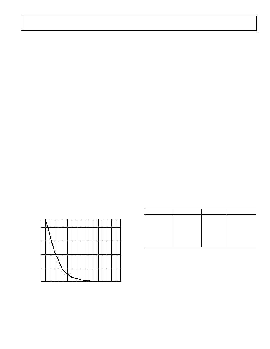
is reprogrammed. Also, note that retention lifetime, based on
an activation energy of 0.6 eV, derates with TJ, as shown in
0
150
300
450
600
30
40
55
70
85
100
125
135
150
RE
T
E
NT
IO
N
(
Y
ea
rs
)
JUNCTION TEMPERATURE (°C)
05
98
6-
01
2
Figure 12. Flash/EE Memory Data Retention
CODE EXECUTION TIME FROM SRAM AND FLASH/EE
This section describes SRAM and Flash/EE memory access times
during execution for applications where execution time is critical.
Execution from SRAM
Fetching instructions from SRAM takes one clock cycle.
However, if the instruction involves reading or writing data to
memory, one or two extra cycles must be added. If the data is in
SRAM, one extra cycle is needed. If the data is in Flash/EE, two
extra cycles are needed to get the 32-bit data from Flash/EE.
A control flow instruction (for example, a branch instruction)
takes one cycle to fetch and two cycles to fill the pipeline with the
new instructions.
Execution from Flash/EE
In Thumb mode, where instructions are 16 bits, one cycle is
needed to fetch any instruction.
In ARM mode, with CD = 0, two cycles are needed to fetch the
32-bit instructions. With CD > 0, no extra cycles are required
for the fetch because the Flash/EE memory continues to be
clocked at full speed. In addition, some dead time is needed
before accessing data for any value of CD bits.
Timing is identical in both modes when executing instructions
that involve using the Flash/EE for data memory. If the instruction
to be executed is a control flow instruction, an extra cycle is
needed to decode the new address of the program counter, and
then four cycles are needed to fill the pipeline if CD = 0.
A data processing instruction involving only the core register
does not require any extra clock cycles. Data transfer instructions
are more complex and are summarized in Table 19.
Table 19. Typical Execution Cycles in ARM/Thumb Mode
Instruction
Fetch Cycle
Dead Time
Data Access
LD
2/1
1
2
LDH
2/1
1
LDM/POP
2/1
N
2 × N
STR
2/1
1
2 × 50 μs
STRH
2/1
1
50 μs
STM/PUSH
2/1
N
2 × N × 50 μs
With 1 < N ≤ 16, N is the number of registers to load or store in
the multiple load/store instruction.
By default, Flash/EE code execution is suspended during any
Flash/EE erase or write cycle. A page (512 bytes) erase cycle
takes 20 ms, and a write (16 bits) word command takes 50 μs.
However, the Flash/EE memory controller allows erase/write
cycles to be aborted if the ARM core receives an enabled interrupt
during the current Flash/EE erase/write cycle. The ARM7 can,
therefore, immediately service the interrupt and then return to
repeat the Flash/EE command. The abort operation typically
takes 10 clock cycles. If the abort operation is not feasible, it is
possible to run Flash/EE memory programming code and the
relevant interrupt routines from SRAM, allowing the core to
service the interrupt immediately.
相关PDF资料 |
PDF描述 |
|---|---|
| AT91R40008-66AU-999 | IC MCU 32BIT RISC 100LQFP |
| ADUC7024BSTZ62-RL | IC MCU 12BIT 1MSPS UART 64-LQFP |
| VE-B33-IW-F3 | CONVERTER MOD DC/DC 24V 100W |
| VE-B33-IW-F1 | CONVERTER MOD DC/DC 24V 100W |
| VE-B34-IX-F3 | CONVERTER MOD DC/DC 48V 75W |
相关代理商/技术参数 |
参数描述 |
|---|---|
| ADUC7032BSTZ-8L | 制造商:Analog Devices 功能描述:FLASH 96K ARM7 TRIPLE 16-BIT ADC LIN IC. - Trays |
| ADUC7032BSTZ-8L-RL | 制造商:Analog Devices 功能描述:FLASH 96K ARM7 TRIPLE 16-BIT ADC LIN IC. - Tape and Reel |
| ADUC7032BSTZ-8V | 制造商:Analog Devices 功能描述: 制造商:Rochester Electronics LLC 功能描述: |
| ADUC7032BSTZ-8V-RL | 功能描述:IC BATTERY SENSOR PREC 48-LQFP RoHS:是 类别:集成电路 (IC) >> 嵌入式 - 微控制器, 系列:MicroConverter® ADuC7xxx 标准包装:1,500 系列:AVR® ATtiny 核心处理器:AVR 芯体尺寸:8-位 速度:16MHz 连通性:I²C,LIN,SPI,UART/USART,USI 外围设备:欠压检测/复位,POR,PWM,温度传感器,WDT 输入/输出数:16 程序存储器容量:8KB(4K x 16) 程序存储器类型:闪存 EEPROM 大小:512 x 8 RAM 容量:512 x 8 电压 - 电源 (Vcc/Vdd):2.7 V ~ 5.5 V 数据转换器:A/D 11x10b 振荡器型:内部 工作温度:-40°C ~ 125°C 封装/外壳:20-SOIC(0.295",7.50mm 宽) 包装:带卷 (TR) |
| ADUC7033 | 制造商:AD 制造商全称:Analog Devices 功能描述:Integrated Precision Battery Sensor For Automotive |
发布紧急采购,3分钟左右您将得到回复。