- 您现在的位置:买卖IC网 > PDF目录11203 > ADUC7032BSTZ-88-RL (Analog Devices Inc)IC MCU 96K FLASH DUAL 48LQFP PDF资料下载
参数资料
| 型号: | ADUC7032BSTZ-88-RL |
| 厂商: | Analog Devices Inc |
| 文件页数: | 89/120页 |
| 文件大小: | 0K |
| 描述: | IC MCU 96K FLASH DUAL 48LQFP |
| 标准包装: | 2,000 |
| 系列: | MicroConverter® ADuC7xxx |
| 核心处理器: | ARM7 |
| 芯体尺寸: | 16/32-位 |
| 速度: | 20.48MHz |
| 连通性: | LIN,SPI,UART/USART |
| 外围设备: | POR,PSM,温度传感器,WDT |
| 输入/输出数: | 9 |
| 程序存储器容量: | 96KB(48K x 16) |
| 程序存储器类型: | 闪存 |
| RAM 容量: | 1.5K x 32 |
| 电压 - 电源 (Vcc/Vdd): | 3.5 V ~ 18 V |
| 数据转换器: | A/D 2x16b |
| 振荡器型: | 内部 |
| 工作温度: | -40°C ~ 105°C |
| 封装/外壳: | 48-LQFP |
| 包装: | 带卷 (TR) |
第1页第2页第3页第4页第5页第6页第7页第8页第9页第10页第11页第12页第13页第14页第15页第16页第17页第18页第19页第20页第21页第22页第23页第24页第25页第26页第27页第28页第29页第30页第31页第32页第33页第34页第35页第36页第37页第38页第39页第40页第41页第42页第43页第44页第45页第46页第47页第48页第49页第50页第51页第52页第53页第54页第55页第56页第57页第58页第59页第60页第61页第62页第63页第64页第65页第66页第67页第68页第69页第70页第71页第72页第73页第74页第75页第76页第77页第78页第79页第80页第81页第82页第83页第84页第85页第86页第87页第88页当前第89页第90页第91页第92页第93页第94页第95页第96页第97页第98页第99页第100页第101页第102页第103页第104页第105页第106页第107页第108页第109页第110页第111页第112页第113页第114页第115页第116页第117页第118页第119页第120页
ADuC7032-8L
Rev. A | Page 70 of 120
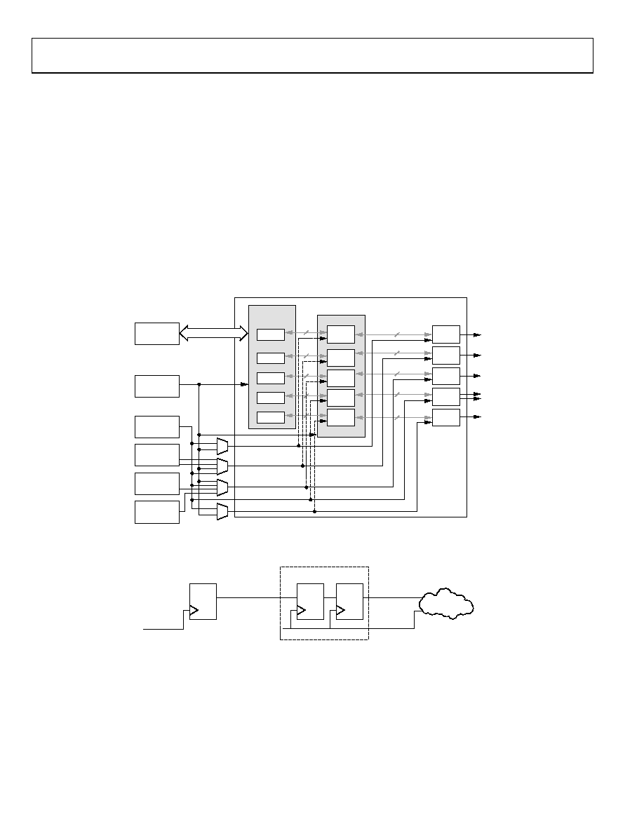
SYNCHRONIZATION OF TIMERS ACROSS
ASYNCHRONOUS CLOCK DOMAINS
The block diagram in Figure 30 shows the interface between
user timer MMRs and the core timer blocks. User code can
access all timer MMRs directly, including TxLD, TxVAL,
TxCON, and TxCLRI. Data must then transfer from these
MMRs to the core timers (T0, T1, T2, T3, and T4) within the
timer subsystem. Theses core timers are buffered from the
user MMR interface by the synchronization (SYNC) block.
The principal of the SYNC block is to provide a method that
ensures that data and other required control signals can cross
asynchronous clock domains correctly. An example of asyn-
chronous clock domains is the MCU running on the 10 MHz
core clock, and Timer2 running on the low power oscillator
of 32 kHz.
As shown in Figure 30, the MMR logic and core timer logic
reside in separate and asynchronous clock domains. Any data
coming from the MMR core clock domain and being passed to
the internal timer domain must be synchronized to the internal
timer clock domain to ensure it is latched correctly into the core
timer clock domain. This is achieved by using two flip-flops, as
shown in Figure 31, to not only synchronize, but also to double
buffer the data and thereby ensure data integrity in the timer
clock domain.
As a result of the synchronization block, while timer control
data is latched almost immediately (with the fast, core clock) in
the MMR clock domain, this data in turn does not reach the
core timer logic for at least two periods of the selected internal
timer domain clock.
T0
SYNC
T1
SYNC
T2
SYNC
T3
SYNC
T4
SYNC
T0
T1
T2
T3
T4
T0IRQ
T1IRQ
T2IRQ
T3IRQ
WdRst
T4IRQ
T0 REG
USER
MMR
INTERFACE
T1 REG
T2 REG
T3 REG
T4 REG
CORE
CLOCK
ARM7TDMI
AMBA
LOW
POWER
OSCILLATOR
HIGH
PRECISION
OSCILLATOR
GPIO
XTAL
0
1
2
4
AMBA
TIMER BLOCK
059
86
-058
Figure 30. Timer Block Diagram
UNSYNCHRONIZED
SIGNAL
SYNCHRONIZED
SIGNAL
TIMER 2
LOW POWER
CLOCK DOMAIN
SYNCHRONIZER
FLIP-FLOPS
CORE CLOCK
(FCORE)
DOMAIN
TARGET_CLOCK
0
598
6-
0
59
Figure 31. Synchronizer for Signals Crossing Clock Domains
相关PDF资料 |
PDF描述 |
|---|---|
| AT91R40008-66AU-999 | IC MCU 32BIT RISC 100LQFP |
| ADUC7024BSTZ62-RL | IC MCU 12BIT 1MSPS UART 64-LQFP |
| VE-B33-IW-F3 | CONVERTER MOD DC/DC 24V 100W |
| VE-B33-IW-F1 | CONVERTER MOD DC/DC 24V 100W |
| VE-B34-IX-F3 | CONVERTER MOD DC/DC 48V 75W |
相关代理商/技术参数 |
参数描述 |
|---|---|
| ADUC7032BSTZ-8L | 制造商:Analog Devices 功能描述:FLASH 96K ARM7 TRIPLE 16-BIT ADC LIN IC. - Trays |
| ADUC7032BSTZ-8L-RL | 制造商:Analog Devices 功能描述:FLASH 96K ARM7 TRIPLE 16-BIT ADC LIN IC. - Tape and Reel |
| ADUC7032BSTZ-8V | 制造商:Analog Devices 功能描述: 制造商:Rochester Electronics LLC 功能描述: |
| ADUC7032BSTZ-8V-RL | 功能描述:IC BATTERY SENSOR PREC 48-LQFP RoHS:是 类别:集成电路 (IC) >> 嵌入式 - 微控制器, 系列:MicroConverter® ADuC7xxx 标准包装:1,500 系列:AVR® ATtiny 核心处理器:AVR 芯体尺寸:8-位 速度:16MHz 连通性:I²C,LIN,SPI,UART/USART,USI 外围设备:欠压检测/复位,POR,PWM,温度传感器,WDT 输入/输出数:16 程序存储器容量:8KB(4K x 16) 程序存储器类型:闪存 EEPROM 大小:512 x 8 RAM 容量:512 x 8 电压 - 电源 (Vcc/Vdd):2.7 V ~ 5.5 V 数据转换器:A/D 11x10b 振荡器型:内部 工作温度:-40°C ~ 125°C 封装/外壳:20-SOIC(0.295",7.50mm 宽) 包装:带卷 (TR) |
| ADUC7033 | 制造商:AD 制造商全称:Analog Devices 功能描述:Integrated Precision Battery Sensor For Automotive |
发布紧急采购,3分钟左右您将得到回复。