- 您现在的位置:买卖IC网 > PDF目录11720 > ADUC832BCPZ (Analog Devices Inc)IC MCU 62K FLASH ADC/DAC 56LFCSP PDF资料下载
参数资料
| 型号: | ADUC832BCPZ |
| 厂商: | Analog Devices Inc |
| 文件页数: | 27/92页 |
| 文件大小: | 0K |
| 描述: | IC MCU 62K FLASH ADC/DAC 56LFCSP |
| 标准包装: | 1 |
| 系列: | MicroConverter® ADuC8xx |
| 核心处理器: | 8052 |
| 芯体尺寸: | 8-位 |
| 速度: | 16MHz |
| 连通性: | EBI/EMI,I²C,SPI,UART/USART |
| 外围设备: | PSM,温度传感器,WDT |
| 输入/输出数: | 34 |
| 程序存储器容量: | 62KB(62K x 8) |
| 程序存储器类型: | 闪存 |
| EEPROM 大小: | 4K x 8 |
| RAM 容量: | 2.25K x 8 |
| 电压 - 电源 (Vcc/Vdd): | 2.7 V ~ 5.5 V |
| 数据转换器: | A/D 8x12b,D/A 2x12b |
| 振荡器型: | 内部 |
| 工作温度: | -40°C ~ 85°C |
| 封装/外壳: | 56-VFQFN 裸露焊盘,CSP |
| 包装: | 托盘 |
第1页第2页第3页第4页第5页第6页第7页第8页第9页第10页第11页第12页第13页第14页第15页第16页第17页第18页第19页第20页第21页第22页第23页第24页第25页第26页当前第27页第28页第29页第30页第31页第32页第33页第34页第35页第36页第37页第38页第39页第40页第41页第42页第43页第44页第45页第46页第47页第48页第49页第50页第51页第52页第53页第54页第55页第56页第57页第58页第59页第60页第61页第62页第63页第64页第65页第66页第67页第68页第69页第70页第71页第72页第73页第74页第75页第76页第77页第78页第79页第80页第81页第82页第83页第84页第85页第86页第87页第88页第89页第90页第91页第92页
Data Sheet
ADuC832
Rev. B | Page 33 of 92
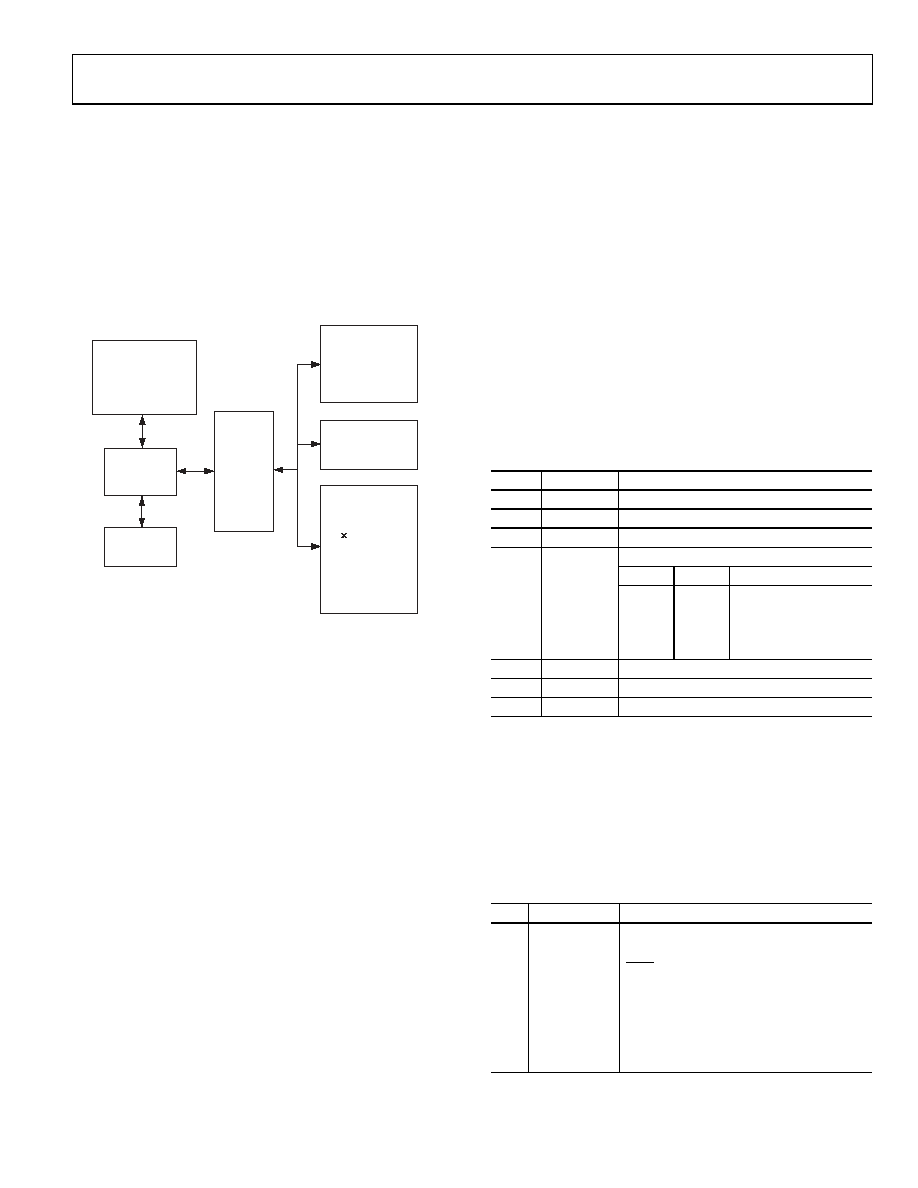
SPECIAL FUNCTION REGISTERS (SFRS)
The SFR space is mapped into the upper 128 bytes of internal
data memory space and accessed by direct addressing only.
It provides an interface between the CPU and all on-chip peripher-
als. A block diagram showing the programming model of the
ADuC832 via the SFR area is shown in Figure 35.
All registers, except the program counter (PC) and the four
general-purpose register banks, reside in the SFR area. The SFR
registers include control, configuration, and data registers that
provide an interface between the CPU and all on-chip peripherals.
128-BYTE
SPECIAL
FUNCTION
REGISTER
AREA
62-kB
ELECTRICALLY
REPROGRAMMABLE
NONVOLATILE
FLASH/EE PROGRAM
MEMORY
8051-
COMPATIBLE
CORE
OTHER ON-CHIP
PERIPHERALS
TEMPERATURE
SENSOR
2
12-BIT DACs
SERIAL I/O
WDT
PSM
TIC
PWM
8-CHANNEL
12-BIT ADC
4-kB
ELECTRICALLY
REPROGRAMMABLE
NONVOLATILE
FLASH/EE DATA
MEMORY
2304 BYTES
RAM
02987-
024
Figure 35. Programming Model
ACCUMULATOR SFR (ACC)
ACC is the accumulator register and is used for math operations
including addition, subtraction, integer multiplication and
division, and Boolean bit manipulations. The mnemonics for
accumulator-specific instructions refer to the accumulator as A.
B SFR (B)
The B register is used with the ACC for multiplication and
division operations. For other instructions, it can be treated
as a general-purpose scratch pad register.
STACK POINTER (SP AND SPH)
The SP SFR is the stack pointer and is used to hold an internal
RAM address that is called the top of the stack. The SP register
is incremented before data is stored during push and call
executions. While the stack may reside anywhere in on-chip
RAM, the SP register is initialized to 07H after a reset. This
causes the stack to begin at Location 08H.
As mentioned previously, the ADuC832 offers an extended
11-bit stack pointer. The three extra bits to make up the 11-bit
stack pointer are the three LSBs of the SPH byte located at B7H.
DATA POINTER (DPTR)
The data pointer is made up of three 8-bit registers, named DPP
(page byte), DPH (high byte), and DPL (low byte). These are
used to provide memory addresses for internal and external
code access and external data access. It can be manipulated as a
16-bit register (DPTR = DPH, DPL), although INC DPTR
instructions automatically carry over to DPP, or as three
independent 8-bit registers (DPP, DPH, and DPL).
The ADuC832 supports dual data pointers. Refer to the Dual
Data Pointers section.
PROGRAM STATUS WORD (PSW)
SFR Address:
D0H
Power-On Default Value:
00H
Bit Addressable:
Yes
The PSW SFR contains several bits reflecting the current status
of the CPU, as detailed in Table 14.
Table 14. PSW SFR Bit Designations
Bit
Name
Description
[7]
CY
Carry flag
[6]
AC
Auxiliary carry flag
[5]
F0
General-purpose flag
[4:3]
RS[1:0]
Register bank select bits
RS1
RS0
Selected Bank
0
1
0
2
1
3
[2]
OV
Overflow flag
[1]
F1
General-purpose flag
[0]
P
Parity bit
POWER CONTROL SFR (PCON)
SFR Address:
87H
Power-On Default Value:
00H
Bit Addressable:
No
The PCON SFR contains bits for power-saving options and
general-purpose status flags, as shown in Table 15.
Table 15. PCON SFR Bit Designations
Bit
Name
Description
[7]
SMOD
Double UART baud rate
[6]
SERIPD
I2C/SPI power-down interrupt enable
[5]
INT0PD
INT0 power-down interrupt enable
[4]
ALEOFF
Disable ALE output
[3]
GF1
General-purpose flag bit
[2]
GF0
General-purpose flag bit
[1]
PD
Power-down mode enable
[0]
IDL
Idle mode enable
相关PDF资料 |
PDF描述 |
|---|---|
| 31-10 | BNC FRONT MOUNT RECEPT |
| D38999/20JD97SN | CONN RCPT 12POS WALL MNT W/SCKT |
| ADUC848BSZ62-5 | IC FLASH MCU W/16BIT ADC 52MQFP |
| ADUC847BSZ32-5 | IC FLASH MCU W/24BIT ADC 52-MQFP |
| D38999/20WD97SB | CONN RCPT 12POS WALL MNT W/SCKT |
相关代理商/技术参数 |
参数描述 |
|---|---|
| ADUC832BCPZ-REEL | 功能描述:IC MCU 62K FLASH ADC/DAC 56LFCSP RoHS:是 类别:集成电路 (IC) >> 嵌入式 - 微控制器, 系列:MicroConverter® ADuC8xx 标准包装:38 系列:Encore!® XP® 核心处理器:eZ8 芯体尺寸:8-位 速度:5MHz 连通性:IrDA,UART/USART 外围设备:欠压检测/复位,LED,POR,PWM,WDT 输入/输出数:16 程序存储器容量:4KB(4K x 8) 程序存储器类型:闪存 EEPROM 大小:- RAM 容量:1K x 8 电压 - 电源 (Vcc/Vdd):2.7 V ~ 3.6 V 数据转换器:- 振荡器型:内部 工作温度:-40°C ~ 105°C 封装/外壳:20-SOIC(0.295",7.50mm 宽) 包装:管件 其它名称:269-4116Z8F0413SH005EG-ND |
| ADUC832BS | 制造商:Analog Devices 功能描述:MCU 8-Bit ADuC8xx 8052 CISC 62KB Flash 3.3V/5V 52-Pin MQFP 制造商:Rochester Electronics LLC 功能描述:8BIT CISC 62KB FLASH 16.78MHZ 3.3/5V 52MQFP - Bulk 制造商:Analog Devices 功能描述:8BIT MCU +12BIT ADC LQFP52 832 |
| ADUC832BS-REEL | 制造商:Analog Devices 功能描述:MCU 8-Bit ADuC8xx 8052 CISC 62KB Flash 3.3V/5V 52-Pin MQFP T/R |
| ADUC832BSZ | 功能描述:IC ADC/DAC 12BIT W/MCU 52MQFP RoHS:是 类别:集成电路 (IC) >> 嵌入式 - 微控制器, 系列:MicroConverter® ADuC8xx 标准包装:250 系列:56F8xxx 核心处理器:56800E 芯体尺寸:16-位 速度:60MHz 连通性:CAN,SCI,SPI 外围设备:POR,PWM,温度传感器,WDT 输入/输出数:21 程序存储器容量:40KB(20K x 16) 程序存储器类型:闪存 EEPROM 大小:- RAM 容量:6K x 16 电压 - 电源 (Vcc/Vdd):2.25 V ~ 3.6 V 数据转换器:A/D 6x12b 振荡器型:内部 工作温度:-40°C ~ 125°C 封装/外壳:48-LQFP 包装:托盘 配用:MC56F8323EVME-ND - BOARD EVALUATION MC56F8323 |
| ADUC832BSZ-REEL | 功能描述:IC MCU 62K FLASH ADC/DAC 52MQFP RoHS:是 类别:集成电路 (IC) >> 嵌入式 - 微控制器, 系列:MicroConverter® ADuC8xx 标准包装:38 系列:Encore!® XP® 核心处理器:eZ8 芯体尺寸:8-位 速度:5MHz 连通性:IrDA,UART/USART 外围设备:欠压检测/复位,LED,POR,PWM,WDT 输入/输出数:16 程序存储器容量:4KB(4K x 8) 程序存储器类型:闪存 EEPROM 大小:- RAM 容量:1K x 8 电压 - 电源 (Vcc/Vdd):2.7 V ~ 3.6 V 数据转换器:- 振荡器型:内部 工作温度:-40°C ~ 105°C 封装/外壳:20-SOIC(0.295",7.50mm 宽) 包装:管件 其它名称:269-4116Z8F0413SH005EG-ND |
发布紧急采购,3分钟左右您将得到回复。