- 您现在的位置:买卖IC网 > PDF目录11720 > ADUC832BCPZ (Analog Devices Inc)IC MCU 62K FLASH ADC/DAC 56LFCSP PDF资料下载
参数资料
| 型号: | ADUC832BCPZ |
| 厂商: | Analog Devices Inc |
| 文件页数: | 37/92页 |
| 文件大小: | 0K |
| 描述: | IC MCU 62K FLASH ADC/DAC 56LFCSP |
| 标准包装: | 1 |
| 系列: | MicroConverter® ADuC8xx |
| 核心处理器: | 8052 |
| 芯体尺寸: | 8-位 |
| 速度: | 16MHz |
| 连通性: | EBI/EMI,I²C,SPI,UART/USART |
| 外围设备: | PSM,温度传感器,WDT |
| 输入/输出数: | 34 |
| 程序存储器容量: | 62KB(62K x 8) |
| 程序存储器类型: | 闪存 |
| EEPROM 大小: | 4K x 8 |
| RAM 容量: | 2.25K x 8 |
| 电压 - 电源 (Vcc/Vdd): | 2.7 V ~ 5.5 V |
| 数据转换器: | A/D 8x12b,D/A 2x12b |
| 振荡器型: | 内部 |
| 工作温度: | -40°C ~ 85°C |
| 封装/外壳: | 56-VFQFN 裸露焊盘,CSP |
| 包装: | 托盘 |
第1页第2页第3页第4页第5页第6页第7页第8页第9页第10页第11页第12页第13页第14页第15页第16页第17页第18页第19页第20页第21页第22页第23页第24页第25页第26页第27页第28页第29页第30页第31页第32页第33页第34页第35页第36页当前第37页第38页第39页第40页第41页第42页第43页第44页第45页第46页第47页第48页第49页第50页第51页第52页第53页第54页第55页第56页第57页第58页第59页第60页第61页第62页第63页第64页第65页第66页第67页第68页第69页第70页第71页第72页第73页第74页第75页第76页第77页第78页第79页第80页第81页第82页第83页第84页第85页第86页第87页第88页第89页第90页第91页第92页
ADuC832
Data Sheet
Rev. B | Page 42 of 92
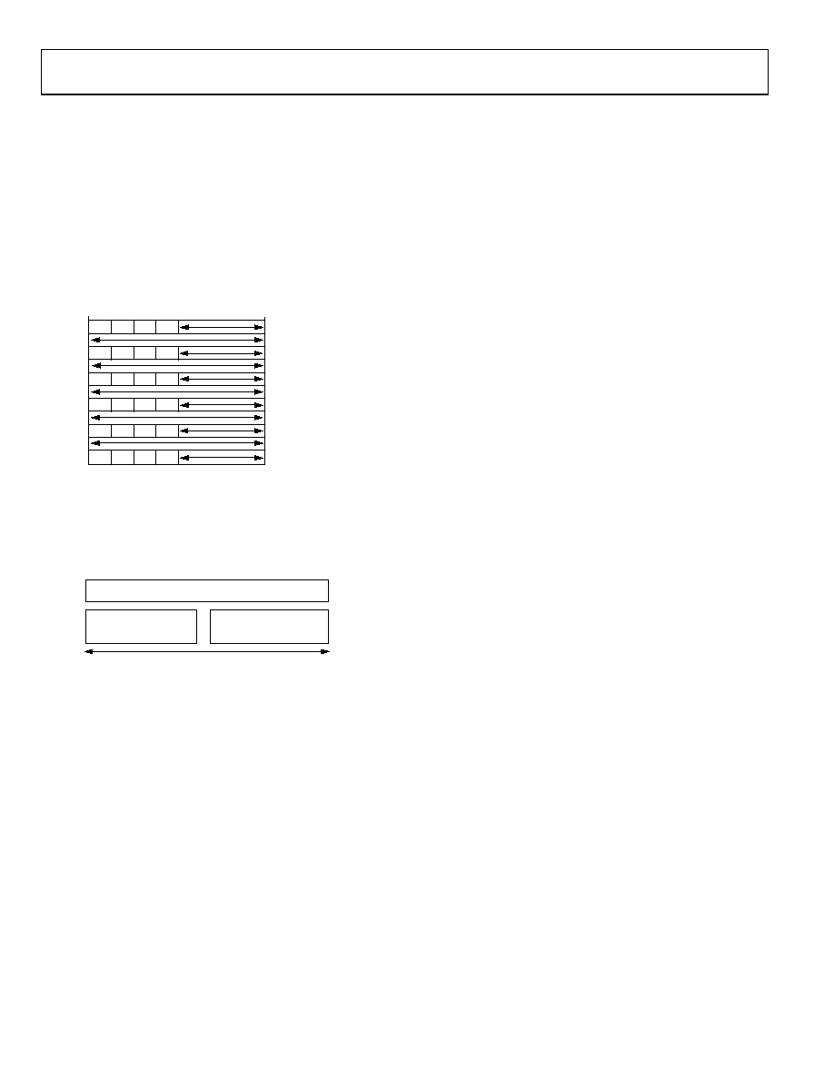
When the DMA conversions are completed, the ADC interrupt
bit, ADCI, is set by hardware and the external SRAM contains
the new ADC conversion results as shown in Figure 45. Note
that no result is written to the last two memory locations.
When the DMA mode logic is active, it takes the responsibility
of storing the ADC results away from both the user and ADuC832
core logic. As it writes the results of the ADC conversions to
external memory, it takes over the external memory interface
from the core. Thus, any core instructions that access the external
memory while DMA mode is enabled do not gain access to it.
The core executes the instructions, which take the same time to
execute, but do not gain access to the external memory.
NO CONVERSION
RESULT WRITTEN HERE
CONVERSION RESULT
FOR ADC CH 3
CONVERSION RESULT
FOR TEMP SENSOR
CONVERSION RESULT
FOR ADC CH 5
CONVERSION RESULT
FOR ADC CH 2
00000AH
000000H
STOP COMMAND
1
0
1
0
1
0
1
0
1
02987-
034
Figure 45. Typical External Memory Configuration Post-ADC DMA Operation
The DMA logic operates from the ADC clock and uses pipelin-
ing to perform the ADC conversions and to access the external
memory at the same time. The time it takes to perform one
ADC conversion is called a DMA cycle. The actions performed
by the logic during a typical DMA cycle are shown in Figure 46.
WRITE ADC RESULT
CONVERTED DURING
PREVIOUS DMA CYCLE
READ CHANNEL ID
TO BE CONVERTED DURING
NEXT DMA CYCLE
CONVERT CHANNEL READ DURING PREVIOUS DMA CYCLE
DMA CYCLE
02987-
035
Figure 46. DMA Cycle
From Figure 46, it can be seen that during one DMA cycle, the
following actions are performed by the DMA logic:
An ADC conversion is performed on the channel whose
ID was read during the previous cycle.
The 12-bit result and the channel ID of the conversion
performed in the previous cycle is written to the external
memory.
The ID of the next channel to be converted is read from
external memory.
For the previous example, the complete flow of events is shown
in Figure 46. Because the DMA logic uses pipelining, it takes
three cycles before the first correct result is written out.
MICRO-OPERATION DURING ADC DMA MODE
During ADC DMA mode, the MicroConverter core is free to
continue code execution, including general housekeeping and
communication tasks. However, note that MCU core accesses to
Port 0 and Port 2 (which are being used by the DMA controller)
are gated off during ADC DMA mode of operation. This means
that even though the instruction that accesses the external Port 0 or
Port 2 appears to execute, no data is seen at these external ports
as a result. Note that during DMA to the internally contained
XRAM, Port 0 and Port 2 are available for use.
The only case in which the MCU is able to access XRAM during
DMA is when the internal XRAM is enabled and the section of
RAM to which the DMA ADC results are being written to lies
in an external XRAM. Then the MCU is able to access only the
internal XRAM. This is also the case for use of the extended
stack pointer.
The MicroConverter core can be configured with an interrupt
to be triggered by the DMA controller when it has finished
filling the requested block of RAM with ADC results, allowing
the service routine for this interrupt to postprocess data without
any real-time timing constraints.
ADC OFFSET AND GAIN CALIBRATION
COEFFICIENTS
The ADuC832 has two ADC calibration coefficients, one for
offset calibration and one for gain calibration. Both the offset
and gain calibration coefficients are 14-bit words, and are each
stored in two registers located in the special function register
(SFR) area. The offset calibration coefficient is divided into
ADCOFSH (six bits) and ADCOFSL (eight bits) and the gain
calibration coefficient is divided into ADCGAINH (six bits)
and ADCGAINL (eight bits).
The offset calibration coefficient compensates for dc offset
errors in both the ADC and the input signal. Increasing the
offset coefficient compensates for positive offset, and effectively
pushes the ADC transfer function down. Decreasing the offset
coefficient compensates for negative offset, and effectively
pushes the ADC transfer function up. The maximum offset that
can be compensated is typically ±5% of VREF, which equates to
typically ±125 mV with a 2.5 V reference.
Similarly, the gain calibration coefficient compensates for dc
gain errors in both the ADC and the input signal. Increasing the
gain coefficient compensates for a smaller analog input signal
range and scales the ADC transfer function up, effectively
increasing the slope of the transfer function. Decreasing the
gain coefficient compensates for a larger analog input signal
range and scales the ADC transfer function down, effectively
decreasing the slope of the transfer function. The maximum
analog input signal range for which the gain coefficient can
compensate is 1.025 × VREF and the minimum input range is
0.975 × VREF, which equates to typically ±2.5% of the reference
voltage.
相关PDF资料 |
PDF描述 |
|---|---|
| 31-10 | BNC FRONT MOUNT RECEPT |
| D38999/20JD97SN | CONN RCPT 12POS WALL MNT W/SCKT |
| ADUC848BSZ62-5 | IC FLASH MCU W/16BIT ADC 52MQFP |
| ADUC847BSZ32-5 | IC FLASH MCU W/24BIT ADC 52-MQFP |
| D38999/20WD97SB | CONN RCPT 12POS WALL MNT W/SCKT |
相关代理商/技术参数 |
参数描述 |
|---|---|
| ADUC832BCPZ-REEL | 功能描述:IC MCU 62K FLASH ADC/DAC 56LFCSP RoHS:是 类别:集成电路 (IC) >> 嵌入式 - 微控制器, 系列:MicroConverter® ADuC8xx 标准包装:38 系列:Encore!® XP® 核心处理器:eZ8 芯体尺寸:8-位 速度:5MHz 连通性:IrDA,UART/USART 外围设备:欠压检测/复位,LED,POR,PWM,WDT 输入/输出数:16 程序存储器容量:4KB(4K x 8) 程序存储器类型:闪存 EEPROM 大小:- RAM 容量:1K x 8 电压 - 电源 (Vcc/Vdd):2.7 V ~ 3.6 V 数据转换器:- 振荡器型:内部 工作温度:-40°C ~ 105°C 封装/外壳:20-SOIC(0.295",7.50mm 宽) 包装:管件 其它名称:269-4116Z8F0413SH005EG-ND |
| ADUC832BS | 制造商:Analog Devices 功能描述:MCU 8-Bit ADuC8xx 8052 CISC 62KB Flash 3.3V/5V 52-Pin MQFP 制造商:Rochester Electronics LLC 功能描述:8BIT CISC 62KB FLASH 16.78MHZ 3.3/5V 52MQFP - Bulk 制造商:Analog Devices 功能描述:8BIT MCU +12BIT ADC LQFP52 832 |
| ADUC832BS-REEL | 制造商:Analog Devices 功能描述:MCU 8-Bit ADuC8xx 8052 CISC 62KB Flash 3.3V/5V 52-Pin MQFP T/R |
| ADUC832BSZ | 功能描述:IC ADC/DAC 12BIT W/MCU 52MQFP RoHS:是 类别:集成电路 (IC) >> 嵌入式 - 微控制器, 系列:MicroConverter® ADuC8xx 标准包装:250 系列:56F8xxx 核心处理器:56800E 芯体尺寸:16-位 速度:60MHz 连通性:CAN,SCI,SPI 外围设备:POR,PWM,温度传感器,WDT 输入/输出数:21 程序存储器容量:40KB(20K x 16) 程序存储器类型:闪存 EEPROM 大小:- RAM 容量:6K x 16 电压 - 电源 (Vcc/Vdd):2.25 V ~ 3.6 V 数据转换器:A/D 6x12b 振荡器型:内部 工作温度:-40°C ~ 125°C 封装/外壳:48-LQFP 包装:托盘 配用:MC56F8323EVME-ND - BOARD EVALUATION MC56F8323 |
| ADUC832BSZ-REEL | 功能描述:IC MCU 62K FLASH ADC/DAC 52MQFP RoHS:是 类别:集成电路 (IC) >> 嵌入式 - 微控制器, 系列:MicroConverter® ADuC8xx 标准包装:38 系列:Encore!® XP® 核心处理器:eZ8 芯体尺寸:8-位 速度:5MHz 连通性:IrDA,UART/USART 外围设备:欠压检测/复位,LED,POR,PWM,WDT 输入/输出数:16 程序存储器容量:4KB(4K x 8) 程序存储器类型:闪存 EEPROM 大小:- RAM 容量:1K x 8 电压 - 电源 (Vcc/Vdd):2.7 V ~ 3.6 V 数据转换器:- 振荡器型:内部 工作温度:-40°C ~ 105°C 封装/外壳:20-SOIC(0.295",7.50mm 宽) 包装:管件 其它名称:269-4116Z8F0413SH005EG-ND |
发布紧急采购,3分钟左右您将得到回复。