- 您现在的位置:买卖IC网 > PDF目录11720 > ADUC832BCPZ (Analog Devices Inc)IC MCU 62K FLASH ADC/DAC 56LFCSP PDF资料下载
参数资料
| 型号: | ADUC832BCPZ |
| 厂商: | Analog Devices Inc |
| 文件页数: | 35/92页 |
| 文件大小: | 0K |
| 描述: | IC MCU 62K FLASH ADC/DAC 56LFCSP |
| 标准包装: | 1 |
| 系列: | MicroConverter® ADuC8xx |
| 核心处理器: | 8052 |
| 芯体尺寸: | 8-位 |
| 速度: | 16MHz |
| 连通性: | EBI/EMI,I²C,SPI,UART/USART |
| 外围设备: | PSM,温度传感器,WDT |
| 输入/输出数: | 34 |
| 程序存储器容量: | 62KB(62K x 8) |
| 程序存储器类型: | 闪存 |
| EEPROM 大小: | 4K x 8 |
| RAM 容量: | 2.25K x 8 |
| 电压 - 电源 (Vcc/Vdd): | 2.7 V ~ 5.5 V |
| 数据转换器: | A/D 8x12b,D/A 2x12b |
| 振荡器型: | 内部 |
| 工作温度: | -40°C ~ 85°C |
| 封装/外壳: | 56-VFQFN 裸露焊盘,CSP |
| 包装: | 托盘 |
第1页第2页第3页第4页第5页第6页第7页第8页第9页第10页第11页第12页第13页第14页第15页第16页第17页第18页第19页第20页第21页第22页第23页第24页第25页第26页第27页第28页第29页第30页第31页第32页第33页第34页当前第35页第36页第37页第38页第39页第40页第41页第42页第43页第44页第45页第46页第47页第48页第49页第50页第51页第52页第53页第54页第55页第56页第57页第58页第59页第60页第61页第62页第63页第64页第65页第66页第67页第68页第69页第70页第71页第72页第73页第74页第75页第76页第77页第78页第79页第80页第81页第82页第83页第84页第85页第86页第87页第88页第89页第90页第91页第92页
ADuC832
Data Sheet
Rev. B | Page 40 of 92
Table 20. Some Single-Supply Op Amps
Op Amp Model
Characteristics
Micropower
I/O Good up to VDD, low cost
I/O to VDD, micropower, low cost
High gain-bandwidth product (GBP)
High GBP, micro package
FET input, low cost
FET input, high GBP
Keep in mind that the ADC’s transfer function is 0 V to VREF,
and any signal range lost to amplifier saturation near ground
impacts dynamic range. Though the op amps in Table 20 are
capable of delivering output signals very closely approaching
ground, no amplifier can deliver signals all the way to ground
when powered by a single supply. Therefore, if a negative supply
is available, consider using it to power the front-end amplifiers.
However, be sure to include the Schottky diodes shown in
Figure 40 (or at least the lower of the two diodes) to protect the
analog input from undervoltage conditions. In summary, use the
circuit of Figure 40 to drive the analog input ADCx pins of the
ADuC832.
VOLTAGE REFERENCE CONNECTIONS
The on-chip 2.5 V band gap voltage reference can be used as
the reference source for the ADC and DACs. To ensure the
accuracy of the voltage reference, the user must decouple the
VREF pin to ground with a 0.1 F capacitor, and the CREF pin to
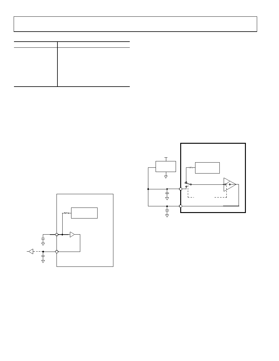
ground with a 0.1 F capacitor, as shown in Figure 41.
BUFFER
0.1F
51
VREF
CREF
2.5V
BAND GAP
REFERENCE
ADuC832
02987-
030
Figure 41. Decoupling VREF and CREF
If the internal voltage reference is to be used as a reference for
external circuitry, the CREF output should be used. However, a
buffer must be used in this case to ensure that no current is
drawn from the CREF pin itself. The voltage on the CREF pin is
that of an internal node within the buffer block, and its voltage
is critical to ADC and DAC accuracy. On the ADuC812, VREF is
the recommended output for the external reference; this can be
used but note that there is a gain error between this reference
and that of the ADC.
The ADuC832 powers up with its internal voltage reference in
the on state. This is available at the VREF pin, but as noted
previously, there is a gain error between this and that of the
ADC. The CREF output becomes available when the ADC is
powered up.
If an external voltage reference is preferred, it should be con-
the ADCCON1 SFR must be set to 1 to switch in the external
reference voltage.
To ensure accurate ADC operation, the voltage applied to VREF
must be between 1 V and AVDD. In situations where analog
input signals are proportional to the power supply (such as
some strain gage applications), it may be desirable to connect
the CREF and VREF pins directly to AVDD.
Operation of the ADC or DACs with a reference voltage below
1 V, however, may incur loss of accuracy, eventually resulting in
missing codes or nonmonotonicity. For that reason, do not use
a reference voltage less than 1 V.
0.1F
51
BUFFER
VREF
CREF
EXTERNAL
VOLTAGE
REFERENCE
1 = EXTERNAL
0 = INTERNAL
2.5V
BAND GAP
REFERENCE
ADuC832
ADCCON1[6]
VDD
02987-
031
Figure 42. Using an External Voltage Reference
To maintain compatibility with the ADuC812, the external
reference can also be connected to the VREF pin, as shown in
Figure 43, to overdrive the internal reference. Note that this
introduces a gain error for the ADC that has to be calibrated
out; thus the previous method is the recommended one for
most users. For this method to work, ADCCON1[6] should be
configured to use the internal reference. The external reference
then overdrives this.
相关PDF资料 |
PDF描述 |
|---|---|
| 31-10 | BNC FRONT MOUNT RECEPT |
| D38999/20JD97SN | CONN RCPT 12POS WALL MNT W/SCKT |
| ADUC848BSZ62-5 | IC FLASH MCU W/16BIT ADC 52MQFP |
| ADUC847BSZ32-5 | IC FLASH MCU W/24BIT ADC 52-MQFP |
| D38999/20WD97SB | CONN RCPT 12POS WALL MNT W/SCKT |
相关代理商/技术参数 |
参数描述 |
|---|---|
| ADUC832BCPZ-REEL | 功能描述:IC MCU 62K FLASH ADC/DAC 56LFCSP RoHS:是 类别:集成电路 (IC) >> 嵌入式 - 微控制器, 系列:MicroConverter® ADuC8xx 标准包装:38 系列:Encore!® XP® 核心处理器:eZ8 芯体尺寸:8-位 速度:5MHz 连通性:IrDA,UART/USART 外围设备:欠压检测/复位,LED,POR,PWM,WDT 输入/输出数:16 程序存储器容量:4KB(4K x 8) 程序存储器类型:闪存 EEPROM 大小:- RAM 容量:1K x 8 电压 - 电源 (Vcc/Vdd):2.7 V ~ 3.6 V 数据转换器:- 振荡器型:内部 工作温度:-40°C ~ 105°C 封装/外壳:20-SOIC(0.295",7.50mm 宽) 包装:管件 其它名称:269-4116Z8F0413SH005EG-ND |
| ADUC832BS | 制造商:Analog Devices 功能描述:MCU 8-Bit ADuC8xx 8052 CISC 62KB Flash 3.3V/5V 52-Pin MQFP 制造商:Rochester Electronics LLC 功能描述:8BIT CISC 62KB FLASH 16.78MHZ 3.3/5V 52MQFP - Bulk 制造商:Analog Devices 功能描述:8BIT MCU +12BIT ADC LQFP52 832 |
| ADUC832BS-REEL | 制造商:Analog Devices 功能描述:MCU 8-Bit ADuC8xx 8052 CISC 62KB Flash 3.3V/5V 52-Pin MQFP T/R |
| ADUC832BSZ | 功能描述:IC ADC/DAC 12BIT W/MCU 52MQFP RoHS:是 类别:集成电路 (IC) >> 嵌入式 - 微控制器, 系列:MicroConverter® ADuC8xx 标准包装:250 系列:56F8xxx 核心处理器:56800E 芯体尺寸:16-位 速度:60MHz 连通性:CAN,SCI,SPI 外围设备:POR,PWM,温度传感器,WDT 输入/输出数:21 程序存储器容量:40KB(20K x 16) 程序存储器类型:闪存 EEPROM 大小:- RAM 容量:6K x 16 电压 - 电源 (Vcc/Vdd):2.25 V ~ 3.6 V 数据转换器:A/D 6x12b 振荡器型:内部 工作温度:-40°C ~ 125°C 封装/外壳:48-LQFP 包装:托盘 配用:MC56F8323EVME-ND - BOARD EVALUATION MC56F8323 |
| ADUC832BSZ-REEL | 功能描述:IC MCU 62K FLASH ADC/DAC 52MQFP RoHS:是 类别:集成电路 (IC) >> 嵌入式 - 微控制器, 系列:MicroConverter® ADuC8xx 标准包装:38 系列:Encore!® XP® 核心处理器:eZ8 芯体尺寸:8-位 速度:5MHz 连通性:IrDA,UART/USART 外围设备:欠压检测/复位,LED,POR,PWM,WDT 输入/输出数:16 程序存储器容量:4KB(4K x 8) 程序存储器类型:闪存 EEPROM 大小:- RAM 容量:1K x 8 电压 - 电源 (Vcc/Vdd):2.7 V ~ 3.6 V 数据转换器:- 振荡器型:内部 工作温度:-40°C ~ 105°C 封装/外壳:20-SOIC(0.295",7.50mm 宽) 包装:管件 其它名称:269-4116Z8F0413SH005EG-ND |
发布紧急采购,3分钟左右您将得到回复。