- 您现在的位置:买卖IC网 > PDF目录11720 > ADUC832BCPZ (Analog Devices Inc)IC MCU 62K FLASH ADC/DAC 56LFCSP PDF资料下载
参数资料
| 型号: | ADUC832BCPZ |
| 厂商: | Analog Devices Inc |
| 文件页数: | 89/92页 |
| 文件大小: | 0K |
| 描述: | IC MCU 62K FLASH ADC/DAC 56LFCSP |
| 标准包装: | 1 |
| 系列: | MicroConverter® ADuC8xx |
| 核心处理器: | 8052 |
| 芯体尺寸: | 8-位 |
| 速度: | 16MHz |
| 连通性: | EBI/EMI,I²C,SPI,UART/USART |
| 外围设备: | PSM,温度传感器,WDT |
| 输入/输出数: | 34 |
| 程序存储器容量: | 62KB(62K x 8) |
| 程序存储器类型: | 闪存 |
| EEPROM 大小: | 4K x 8 |
| RAM 容量: | 2.25K x 8 |
| 电压 - 电源 (Vcc/Vdd): | 2.7 V ~ 5.5 V |
| 数据转换器: | A/D 8x12b,D/A 2x12b |
| 振荡器型: | 内部 |
| 工作温度: | -40°C ~ 85°C |
| 封装/外壳: | 56-VFQFN 裸露焊盘,CSP |
| 包装: | 托盘 |
第1页第2页第3页第4页第5页第6页第7页第8页第9页第10页第11页第12页第13页第14页第15页第16页第17页第18页第19页第20页第21页第22页第23页第24页第25页第26页第27页第28页第29页第30页第31页第32页第33页第34页第35页第36页第37页第38页第39页第40页第41页第42页第43页第44页第45页第46页第47页第48页第49页第50页第51页第52页第53页第54页第55页第56页第57页第58页第59页第60页第61页第62页第63页第64页第65页第66页第67页第68页第69页第70页第71页第72页第73页第74页第75页第76页第77页第78页第79页第80页第81页第82页第83页第84页第85页第86页第87页第88页当前第89页第90页第91页第92页
Data Sheet
ADuC832
Rev. B | Page 9 of 92
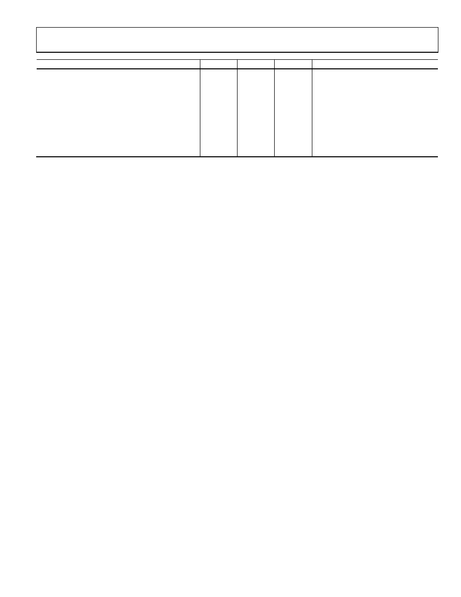
Parameter1
VDD = 5 V
VDD = 3 V
Unit
Test Conditions/Comments
Power Supply Currents Power-Down Mode
Core_CLK = 2.097 MHz or 16.78 MHz
80
25
μA max
Oscillator on
38
14
μA typ
AVDD Current
2
1
μA typ
DVDD Current
35
20
μA max
Oscillator off
25
12
μA typ
Typical Additional Power Supply Currents
AVDD = DVDD = 5 V
PSM Peripheral
50
μA typ
ADC
1.5
mA typ
DAC
150
μA typ
1
Temperature range: 40°C to +125°C.
2
ADC linearity is guaranteed during normal MicroConverter core operation.
3
ADC LSB size = VREF/212, that is, for internal VREF = 2.5 V, 1 LSB = 610 V and for external VREF = 1 V, 1 LSB = 244 V.
4
Not production tested, but are guaranteed by design and/or characterization data on production release.
5
Offset error, gain error, offset error match, and gain error match are measured after factory calibration.
6
Based on external ADC system components, the user may need to execute a system calibration to remove additional external channel errors and achieve these
specifications.
7
SNR calculation includes distortion and noise components.
8
Channel-to-channel crosstalk is measured on adjacent channels.
9
The temperature sensor gives a measure of the die temperature directly; air temperature can be inferred from this result.
10
DAC linearity is calculated using:
Reduced code range of 100 to 4095, 0 V to VREF range.
Reduced code range of 100 to 3945, 0 V to VDD range.
DAC output load = 10 kΩ and 100 pF.
11
DAC differential nonlinearity specified on 0 V to VREF and 0 V to VDD ranges.
12
DAC specification for output impedance in the unbuffered case depends on DAC code.
13
DAC specifications for ISINK, voltage output settling time, and digital-to-analog glitch energy depend on external buffer implementation in unbuffered mode. DAC in
unbuffered mode tested with OP270 external buffer, which has a low input leakage current.
14
Measured with VREF and CREF pins decoupled with 0.1 F capacitors to ground. Power-up time for the internal reference is determined by the value of the decoupling
capacitor chosen for both the VREF and CREF pins.
15
When using an external reference device, the internal band gap reference input can be bypassed by setting the ADCCON1[6] bit. In this mode, the VREF and CREF pins
need to be shorted together for correct operation.
16
Flash/EE Memory reliability characteristics apply to both the Flash/EE program memory and the Flash/EE data memory.
17
Endurance is qualified to 100,000 cycles as per JEDEC Std. 22 method A117 and measured at 40°C, +25°C, and +125°C. Typical endurance at 25°C is 700,000 cycles.
18
Retention lifetime equivalent at junction temperature (TJ) = 55°C as per JEDEC Std. 22 Method A117. Retention lifetime based on an activation energy of 0.6 eV
derates with junction temperature as shown in Figure 48 in the ADuC832 Flash/EE Memory Reliability section.
19
Power supply current consumption is measured in normal, idle, and power-down modes under the following conditions:
Normal mode: RESET = 0.4 V, digital I/O pins = open circuit, Core_CLK changed via the CD bits in PLLCON[2:0], core executing internal software loop.
Idle mode: RESET = 0.4 V, digital I/O pins = open circuit, Core_CLK changed via the CD bits in PLLCON, PCON[0] = 1, core execution suspended in idle mode.
Power-down mode: RESET = 0.4 V, all Port 0 pins = 0.4 V, all other digital I/O and Port 1 pins are open circuit, Core_CLK changed via the CD bits in PLLCON, PCON[1]
= 1, core execution suspended in power-down mode, oscillator turned on or off via OSC_PD bit (PLLCON[7]).
20
DVDD power supply current increases typically by 3 mA (3 V operation) and 10 mA (5 V operation) during a Flash/EE memory program or erase cycle.
相关PDF资料 |
PDF描述 |
|---|---|
| 31-10 | BNC FRONT MOUNT RECEPT |
| D38999/20JD97SN | CONN RCPT 12POS WALL MNT W/SCKT |
| ADUC848BSZ62-5 | IC FLASH MCU W/16BIT ADC 52MQFP |
| ADUC847BSZ32-5 | IC FLASH MCU W/24BIT ADC 52-MQFP |
| D38999/20WD97SB | CONN RCPT 12POS WALL MNT W/SCKT |
相关代理商/技术参数 |
参数描述 |
|---|---|
| ADUC832BCPZ-REEL | 功能描述:IC MCU 62K FLASH ADC/DAC 56LFCSP RoHS:是 类别:集成电路 (IC) >> 嵌入式 - 微控制器, 系列:MicroConverter® ADuC8xx 标准包装:38 系列:Encore!® XP® 核心处理器:eZ8 芯体尺寸:8-位 速度:5MHz 连通性:IrDA,UART/USART 外围设备:欠压检测/复位,LED,POR,PWM,WDT 输入/输出数:16 程序存储器容量:4KB(4K x 8) 程序存储器类型:闪存 EEPROM 大小:- RAM 容量:1K x 8 电压 - 电源 (Vcc/Vdd):2.7 V ~ 3.6 V 数据转换器:- 振荡器型:内部 工作温度:-40°C ~ 105°C 封装/外壳:20-SOIC(0.295",7.50mm 宽) 包装:管件 其它名称:269-4116Z8F0413SH005EG-ND |
| ADUC832BS | 制造商:Analog Devices 功能描述:MCU 8-Bit ADuC8xx 8052 CISC 62KB Flash 3.3V/5V 52-Pin MQFP 制造商:Rochester Electronics LLC 功能描述:8BIT CISC 62KB FLASH 16.78MHZ 3.3/5V 52MQFP - Bulk 制造商:Analog Devices 功能描述:8BIT MCU +12BIT ADC LQFP52 832 |
| ADUC832BS-REEL | 制造商:Analog Devices 功能描述:MCU 8-Bit ADuC8xx 8052 CISC 62KB Flash 3.3V/5V 52-Pin MQFP T/R |
| ADUC832BSZ | 功能描述:IC ADC/DAC 12BIT W/MCU 52MQFP RoHS:是 类别:集成电路 (IC) >> 嵌入式 - 微控制器, 系列:MicroConverter® ADuC8xx 标准包装:250 系列:56F8xxx 核心处理器:56800E 芯体尺寸:16-位 速度:60MHz 连通性:CAN,SCI,SPI 外围设备:POR,PWM,温度传感器,WDT 输入/输出数:21 程序存储器容量:40KB(20K x 16) 程序存储器类型:闪存 EEPROM 大小:- RAM 容量:6K x 16 电压 - 电源 (Vcc/Vdd):2.25 V ~ 3.6 V 数据转换器:A/D 6x12b 振荡器型:内部 工作温度:-40°C ~ 125°C 封装/外壳:48-LQFP 包装:托盘 配用:MC56F8323EVME-ND - BOARD EVALUATION MC56F8323 |
| ADUC832BSZ-REEL | 功能描述:IC MCU 62K FLASH ADC/DAC 52MQFP RoHS:是 类别:集成电路 (IC) >> 嵌入式 - 微控制器, 系列:MicroConverter® ADuC8xx 标准包装:38 系列:Encore!® XP® 核心处理器:eZ8 芯体尺寸:8-位 速度:5MHz 连通性:IrDA,UART/USART 外围设备:欠压检测/复位,LED,POR,PWM,WDT 输入/输出数:16 程序存储器容量:4KB(4K x 8) 程序存储器类型:闪存 EEPROM 大小:- RAM 容量:1K x 8 电压 - 电源 (Vcc/Vdd):2.7 V ~ 3.6 V 数据转换器:- 振荡器型:内部 工作温度:-40°C ~ 105°C 封装/外壳:20-SOIC(0.295",7.50mm 宽) 包装:管件 其它名称:269-4116Z8F0413SH005EG-ND |
发布紧急采购,3分钟左右您将得到回复。