- 您现在的位置:买卖IC网 > PDF目录11720 > ADUC832BCPZ (Analog Devices Inc)IC MCU 62K FLASH ADC/DAC 56LFCSP PDF资料下载
参数资料
| 型号: | ADUC832BCPZ |
| 厂商: | Analog Devices Inc |
| 文件页数: | 65/92页 |
| 文件大小: | 0K |
| 描述: | IC MCU 62K FLASH ADC/DAC 56LFCSP |
| 标准包装: | 1 |
| 系列: | MicroConverter® ADuC8xx |
| 核心处理器: | 8052 |
| 芯体尺寸: | 8-位 |
| 速度: | 16MHz |
| 连通性: | EBI/EMI,I²C,SPI,UART/USART |
| 外围设备: | PSM,温度传感器,WDT |
| 输入/输出数: | 34 |
| 程序存储器容量: | 62KB(62K x 8) |
| 程序存储器类型: | 闪存 |
| EEPROM 大小: | 4K x 8 |
| RAM 容量: | 2.25K x 8 |
| 电压 - 电源 (Vcc/Vdd): | 2.7 V ~ 5.5 V |
| 数据转换器: | A/D 8x12b,D/A 2x12b |
| 振荡器型: | 内部 |
| 工作温度: | -40°C ~ 85°C |
| 封装/外壳: | 56-VFQFN 裸露焊盘,CSP |
| 包装: | 托盘 |
第1页第2页第3页第4页第5页第6页第7页第8页第9页第10页第11页第12页第13页第14页第15页第16页第17页第18页第19页第20页第21页第22页第23页第24页第25页第26页第27页第28页第29页第30页第31页第32页第33页第34页第35页第36页第37页第38页第39页第40页第41页第42页第43页第44页第45页第46页第47页第48页第49页第50页第51页第52页第53页第54页第55页第56页第57页第58页第59页第60页第61页第62页第63页第64页当前第65页第66页第67页第68页第69页第70页第71页第72页第73页第74页第75页第76页第77页第78页第79页第80页第81页第82页第83页第84页第85页第86页第87页第88页第89页第90页第91页第92页
ADuC832
Data Sheet
Rev. B | Page 68 of 92
them drive a logic low output voltage (VOL) and are capable of
sinking 1.6 mA.
P2.6 and P2.7 can also be used as PWM outputs. If they are
selected as the PWM outputs via the CFG832 SFR, the PWM
outputs overwrite anything written to P2.6 or P2.7.
CONTROL
READ
LATCH
INTERNAL
BUS
WRITE
TO LATCH
READ
PIN
D
CL
Q
LATCH
ADDR
P2.x
PIN
INTERNAL
PULL-UP*
*SEE FIGURE 69 FOR
DETAILS OF INTERNAL PULL-UP
DVDD
02987-
057
Q
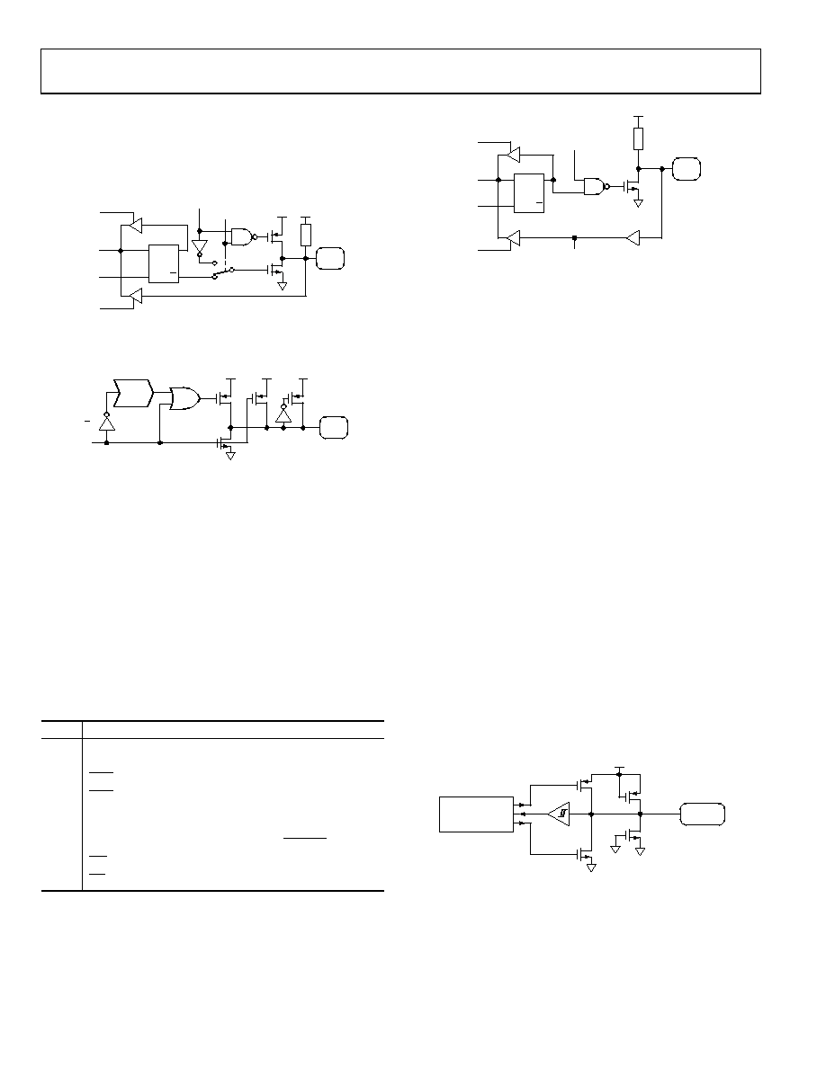
Figure 68. Port 2 Bit Latch and I/O Buffer
Q
FROM
PORT
LATCH
2 CLK
DELAY
Q1
DVDD
Q2
Q3
P2.x
PIN
Q4
DVDD
02987-
058
Figure 69. Internal Pull-Up Configuration
PORT 3
Port 3 is a bidirectional port with internal pull-ups directly
controlled via the P3 SFR. Port 3 pins that have 1s written to
them are pulled high by the internal pull-ups and, in that state,
can be used as inputs. As inputs, Port 3 pins pulled externally
low source current because of the internal pull-ups. Port 3 pins
with 0s written to them drive a logic low output voltage (VOL)
and are capable of sinking 4 mA.
Port 3 pins also have various secondary functions described in
Table 35. The alternate functions of Port 3 pins can only be
activated if the corresponding bit latch in the P3 SFR contains a 1.
Otherwise, the port pin is stuck at 0.
Table 35. Port 3, Alternate Pin Functions
Pin
Alternate Function
P3.0
RxD (UART input pin or serial data I/O in Mode 0)
P3.1
TxD (UART output pin or serial clock output in Mode 0)
P3.2
INT0 (External Interrupt 0)
P3.3
INT1 (External Interrupt 1) or PWM1/MISO
P3.4
T0 (Timer/Counter 0 external input), PWMC, PWM0, or
EXTCLK
P3.5
T1 (Timer/Counter 1 external input) or CONVST
P3.6
WR (external data memory write strobe)
P3.7
RD (external data memory read strobe)
P3.3 and P3.4 can also be used as PWM outputs. If they are
selected as the PWM outputs via the CFG832 SFR, the PWM
outputs overwrite anything written to P3.4 or P3.3.
READ
LATCH
INTERNAL
BUS
WRITE
TO LATCH
READ
PIN
D
CL
Q
LATCH
DVDD
P3.x
PIN
INTERNAL
PULL-UP*
*SEE FIGURE 69
FOR DETAILS OF
INTERNAL PULL-UP
ALTERNATE
OUTPUT
FUNCTION
ALTERNATE
INPUT
FUNCTION
02987-
059
Figure 70. Port 3 Bit Latch and I/O Buffer
ADDITIONAL DIGITAL I/O
In addition to the port pins, the dedicated SPI/I2C pins
(SCLOCK and SDATA/MOSI) also feature both input and
output functions. Their equivalent I/O architectures are
illustrated in Figure 71 and Figure 73, respectively, for SPI
Notice that in I2C mode (SPE, SPICON[5] = 0), the strong pull-
up FET (Q1) is disabled, leaving only a weak pull-up (Q2)
present. By contrast, in SPI mode (SPE = 1) the strong pull-up
FET (Q1) is controlled directly by SPI hardware, giving the pin
push-pull capability.
In I2C mode (SPE = 0), two pull-down FETs (Q3 and Q4)
operate in parallel to provide an extra 60% or 70% of current
sinking capability. In SPI mode, however, (SPE = 1) only one of
the pull-down FETs (Q3) operates on each pin, resulting in sink
capabilities identical to that of Port 0 and Port 2 pins. On the
input path of SCLOCK, notice that a Schmitt trigger conditions
the signal going to the SPI hardware to prevent false triggers
(double triggers) on slow incoming edges. For incoming signals
from the SCLOCK and SDATA pins going to I2C hardware, a filter
conditions the signals in order to reject glitches of up to 50 ns in
duration.
Notice also that direct access to the SCLOCK and SDATA/MOSI
pins is afforded through the SFR interface in I2C master mode.
Therefore, if the SPI or I2C functions are not used, these two
pins can be used to give additional high current digital outputs.
DVDD
HARDWARE SPI
(MASTER/SLAVE)
Q3
SCHMITT
TRIGGER
Q1
Q2 (OFF)
SCLOCK
PIN
Q4 (OFF)
SPE = 1 (SPI ENABLE)
02987-
060
Figure 71. SCLOCK Pin I/O Functional Equivalent in SPI Mode
相关PDF资料 |
PDF描述 |
|---|---|
| 31-10 | BNC FRONT MOUNT RECEPT |
| D38999/20JD97SN | CONN RCPT 12POS WALL MNT W/SCKT |
| ADUC848BSZ62-5 | IC FLASH MCU W/16BIT ADC 52MQFP |
| ADUC847BSZ32-5 | IC FLASH MCU W/24BIT ADC 52-MQFP |
| D38999/20WD97SB | CONN RCPT 12POS WALL MNT W/SCKT |
相关代理商/技术参数 |
参数描述 |
|---|---|
| ADUC832BCPZ-REEL | 功能描述:IC MCU 62K FLASH ADC/DAC 56LFCSP RoHS:是 类别:集成电路 (IC) >> 嵌入式 - 微控制器, 系列:MicroConverter® ADuC8xx 标准包装:38 系列:Encore!® XP® 核心处理器:eZ8 芯体尺寸:8-位 速度:5MHz 连通性:IrDA,UART/USART 外围设备:欠压检测/复位,LED,POR,PWM,WDT 输入/输出数:16 程序存储器容量:4KB(4K x 8) 程序存储器类型:闪存 EEPROM 大小:- RAM 容量:1K x 8 电压 - 电源 (Vcc/Vdd):2.7 V ~ 3.6 V 数据转换器:- 振荡器型:内部 工作温度:-40°C ~ 105°C 封装/外壳:20-SOIC(0.295",7.50mm 宽) 包装:管件 其它名称:269-4116Z8F0413SH005EG-ND |
| ADUC832BS | 制造商:Analog Devices 功能描述:MCU 8-Bit ADuC8xx 8052 CISC 62KB Flash 3.3V/5V 52-Pin MQFP 制造商:Rochester Electronics LLC 功能描述:8BIT CISC 62KB FLASH 16.78MHZ 3.3/5V 52MQFP - Bulk 制造商:Analog Devices 功能描述:8BIT MCU +12BIT ADC LQFP52 832 |
| ADUC832BS-REEL | 制造商:Analog Devices 功能描述:MCU 8-Bit ADuC8xx 8052 CISC 62KB Flash 3.3V/5V 52-Pin MQFP T/R |
| ADUC832BSZ | 功能描述:IC ADC/DAC 12BIT W/MCU 52MQFP RoHS:是 类别:集成电路 (IC) >> 嵌入式 - 微控制器, 系列:MicroConverter® ADuC8xx 标准包装:250 系列:56F8xxx 核心处理器:56800E 芯体尺寸:16-位 速度:60MHz 连通性:CAN,SCI,SPI 外围设备:POR,PWM,温度传感器,WDT 输入/输出数:21 程序存储器容量:40KB(20K x 16) 程序存储器类型:闪存 EEPROM 大小:- RAM 容量:6K x 16 电压 - 电源 (Vcc/Vdd):2.25 V ~ 3.6 V 数据转换器:A/D 6x12b 振荡器型:内部 工作温度:-40°C ~ 125°C 封装/外壳:48-LQFP 包装:托盘 配用:MC56F8323EVME-ND - BOARD EVALUATION MC56F8323 |
| ADUC832BSZ-REEL | 功能描述:IC MCU 62K FLASH ADC/DAC 52MQFP RoHS:是 类别:集成电路 (IC) >> 嵌入式 - 微控制器, 系列:MicroConverter® ADuC8xx 标准包装:38 系列:Encore!® XP® 核心处理器:eZ8 芯体尺寸:8-位 速度:5MHz 连通性:IrDA,UART/USART 外围设备:欠压检测/复位,LED,POR,PWM,WDT 输入/输出数:16 程序存储器容量:4KB(4K x 8) 程序存储器类型:闪存 EEPROM 大小:- RAM 容量:1K x 8 电压 - 电源 (Vcc/Vdd):2.7 V ~ 3.6 V 数据转换器:- 振荡器型:内部 工作温度:-40°C ~ 105°C 封装/外壳:20-SOIC(0.295",7.50mm 宽) 包装:管件 其它名称:269-4116Z8F0413SH005EG-ND |
发布紧急采购,3分钟左右您将得到回复。