参数资料
| 型号: | CDB4245 |
| 厂商: | Cirrus Logic Inc |
| 文件页数: | 38/59页 |
| 文件大小: | 0K |
| 描述: | BOARD EVAL FOR CS4245 CODEC |
| 标准包装: | 1 |
| 主要目的: | 音频编解码器 |
| 嵌入式: | 是,FPGA / CPLD |
| 已用 IC / 零件: | CS4245 |
| 主要属性: | 4 个单端模拟和 1 个麦克风输入和 8 个输出,S/PDIF 发射器和接收器 |
| 次要属性: | 图形用户界面 |
| 已供物品: | 板 |
| 产品目录页面: | 754 (CN2011-ZH PDF) |
| 相关产品: | CS4245-DQZR-ND - IC CODEC AUD STER 104DB 48-LQFP 598-1616-ND - IC CODEC AUD STER 104DB 48LQFP 598-1034-ND - IC CODEC AUD STER 104DB 48LQFP |
| 其它名称: | 598-1501 |
第1页第2页第3页第4页第5页第6页第7页第8页第9页第10页第11页第12页第13页第14页第15页第16页第17页第18页第19页第20页第21页第22页第23页第24页第25页第26页第27页第28页第29页第30页第31页第32页第33页第34页第35页第36页第37页当前第38页第39页第40页第41页第42页第43页第44页第45页第46页第47页第48页第49页第50页第51页第52页第53页第54页第55页第56页第57页第58页第59页
�� �
�
�CS4245�
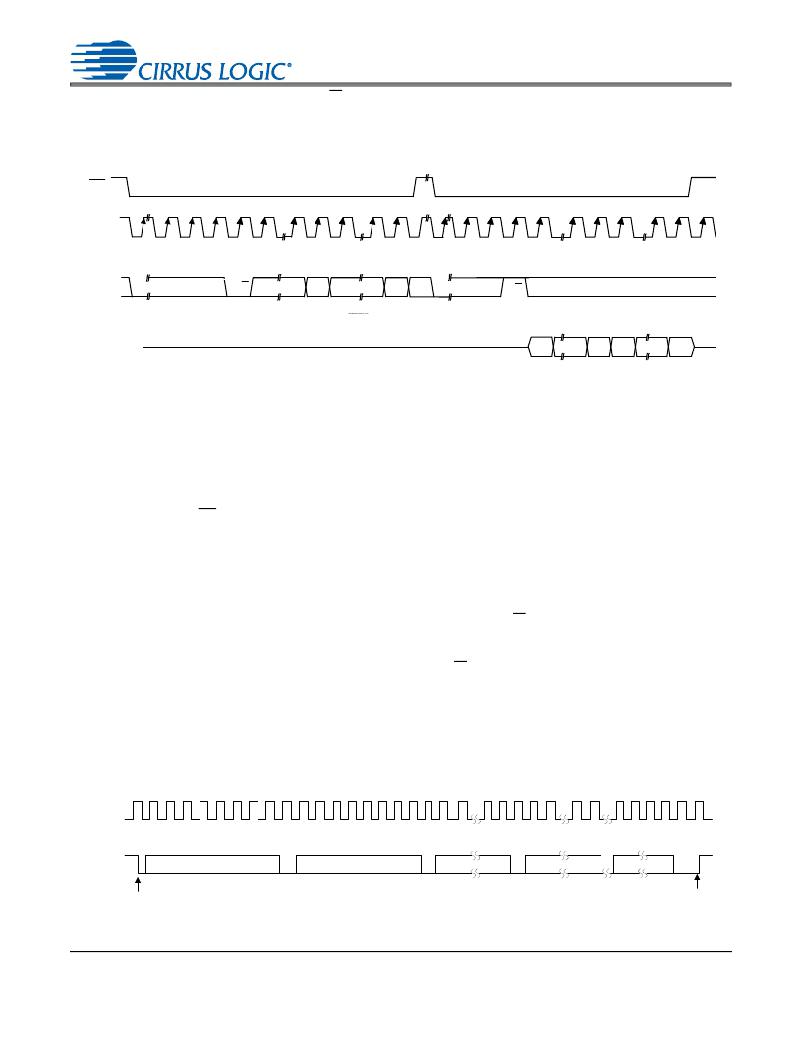
�dress� and� set� the� read/write� bit� (R/W)� high.� The� next� falling� edge� of� CCLK� will� clock� out� the� MSB� of� the�
�addressed� register� (CDOUT� will� leave� the� high-impedance� state).�
�For� both� read� and� write� cycles,� the� memory� address� pointer� will� automatically� increment� following� each�
�data� byte� in� order� to� facilitate� block� reads� and� writes� of� successive� registers.�
�CS�
�CCLK�
�C� H� IP�
�ADDRESS�
�MAP�
�DATA�
�C� H� IP�
�ADDRESS�
�C� D� IN�
�1001111�
�R/W�
�MSB�
�LSB�
�1001111�
�R/W�
�b� y� te� 1�
�b� y� te� n�
�CDOUT�
�High� Impedance�
�MSB�
�LSB MSB�
�LSB�
�MAP� =� Memory� Address� Pointer,� 8� bits,� MSB� first�
�Figure� 17.� Control� Port� Timing� in� SPI� Mode�
�4.12.2� I2C� Mode�
�In� I2C� Mode,� SDA� is� a� bidirectional� data� line.� Data� is� clocked� into� and� out� of� the� part� by� the� clock,� SCL.�
�There� is� no� CS� pin.� Pins� AD0� and� AD1� form� the� two� least-significant� bits� of� the� chip� address� and� should�
�be� connected� through� a� resistor� to� VLC� or� DGND� as� desired.� The� state� of� the� pins� is� sensed� while� the�
�CS4245� is� being� reset.�
�The� signal� timings� for� a� read� and� write� cycle� are� shown� in� Figure� 18� and� Figure� 19� .� A� Start� condition� is�
�defined� as� a� falling� transition� of� SDA� while� the� clock� is� high.� A� Stop� condition� is� a� rising� transition� while�
�the� clock� is� high.� All� other� transitions� of� SDA� occur� while� the� clock� is� low.� The� first� byte� sent� to� the� CS4245�
�after� a� Start� condition� consists� of� a� 7-bit� chip� address� field� and� a� R/W� bit� (high� for� a� read,� low� for� a� write).�
�The� upper� 5� bits� of� the� 7-bit� address� field� are� fixed� at� 10011.� To� communicate� with� a� CS4245,� the� chip�
�address� field,� which� is� the� first� byte� sent� to� the� CS4245,� should� match� 10011� followed� by� the� settings� of�
�the� AD1� and� AD0.� The� eighth� bit� of� the� address� is� the� R/W� bit.� If� the� operation� is� a� write,� the� next� byte� is�
�the� Memory� Address� Pointer� (MAP)� which� selects� the� register� to� be� read� or� written.� If� the� operation� is� a�
�read,� the� contents� of� the� register� pointed� to� by� the� MAP� will� be� output.� Following� each� data� byte,� the� mem-�
�ory� address� pointer� will� automatically� increment� to� facilitate� block� reads� and� writes� of� successive� regis-�
�ters.� Each� byte� is� separated� by� an� acknowledge� bit.� The� ACK� bit� is� output� from� the� CS4245� after� each�
�input� byte� is� read,� and� is� input� to� the� CS4245� from� the� microcontroller� after� each� transmitted� byte.�
�0�
�1�
�2�
�3�
�4�
�5�
�6�
�7�
�8�
�9�
�10� 11� 12� 13� 14� 15� 16� 17� 18�
�19�
�24� 25� 26� 27� 28�
�SCL�
�CHIP� ADDRESS� (WRITE)�
�MAP� BYTE�
�DATA�
�DATA� +1�
�DATA� +n�
�SDA�
�1�
�0�
�0�
�1�
�1� AD1� AD0� 0�
�6�
�6�
�5�
�4�
�3�
�2�
�1�
�0�
�7�
�6�
�1�
�0�
�7�
�6�
�1�
�0�
�7�
�6�
�1�
�0�
�START�
�ACK�
�ACK�
�ACK�
�ACK�
�STOP�
�Figure� 18.� Control� Port� Timing,� I2C� Write�
�38�
�DS656F3�
�相关PDF资料 |
PDF描述 |
|---|---|
| CDB42L55 | BOARD EVAL FOR CS42L55 CODEC |
| CDB44L11 | EVALUATION BOARD FOR CS44L11 |
| CDB48500-USB | KIT USB EVALUATION FOR CDB48500 |
| CDB5378 | EVALUATION BOARD FOR CS5378 |
| CDB5460AU | EVALUATION BOARD FOR CS5460A |
相关代理商/技术参数 |
参数描述 |
|---|---|
| CDB42518 | 功能描述:音频 IC 开发工具 Eval Bd RoHS:否 制造商:Texas Instruments 产品:Evaluation Kits 类型:Audio Amplifiers 工具用于评估:TAS5614L 工作电源电压:12 V to 38 V |
| CDB42528 | 功能描述:音频 IC 开发工具 Eval Bd RoHS:否 制造商:Texas Instruments 产品:Evaluation Kits 类型:Audio Amplifiers 工具用于评估:TAS5614L 工作电源电压:12 V to 38 V |
| CDB4265 | 功能描述:音频 IC 开发工具 Eval Bd 192kHz CODEC w/PGA & Input Mux RoHS:否 制造商:Texas Instruments 产品:Evaluation Kits 类型:Audio Amplifiers 工具用于评估:TAS5614L 工作电源电压:12 V to 38 V |
| CDB4270 | 功能描述:音频 IC 开发工具 Eval Bd 105dB 192kHz CODEC RoHS:否 制造商:Texas Instruments 产品:Evaluation Kits 类型:Audio Amplifiers 工具用于评估:TAS5614L 工作电源电压:12 V to 38 V |
| CDB4271 | 功能描述:音频 IC 开发工具 Eval Bd CS4271 RoHS:否 制造商:Texas Instruments 产品:Evaluation Kits 类型:Audio Amplifiers 工具用于评估:TAS5614L 工作电源电压:12 V to 38 V |
发布紧急采购,3分钟左右您将得到回复。