- 您现在的位置:买卖IC网 > PDF目录295374 > CY7C1248KV18-400BZXC (CYPRESS SEMICONDUCTOR CORP) 2M X 18 DDR SRAM, 0.45 ns, PBGA165 PDF资料下载
参数资料
| 型号: | CY7C1248KV18-400BZXC |
| 厂商: | CYPRESS SEMICONDUCTOR CORP |
| 元件分类: | SRAM |
| 英文描述: | 2M X 18 DDR SRAM, 0.45 ns, PBGA165 |
| 封装: | 13 X 15 MM, 1.40 MM HEIGHT, LEAD FREE, MO-216, FBGA-165 |
| 文件页数: | 17/28页 |
| 文件大小: | 907K |
| 代理商: | CY7C1248KV18-400BZXC |
第1页第2页第3页第4页第5页第6页第7页第8页第9页第10页第11页第12页第13页第14页第15页第16页当前第17页第18页第19页第20页第21页第22页第23页第24页第25页第26页第27页第28页
CY7C1246KV18, CY7C1257KV18
CY7C1248KV18, CY7C1250KV18
Document Number: 001-57834 Rev. *B
Page 24 of 28
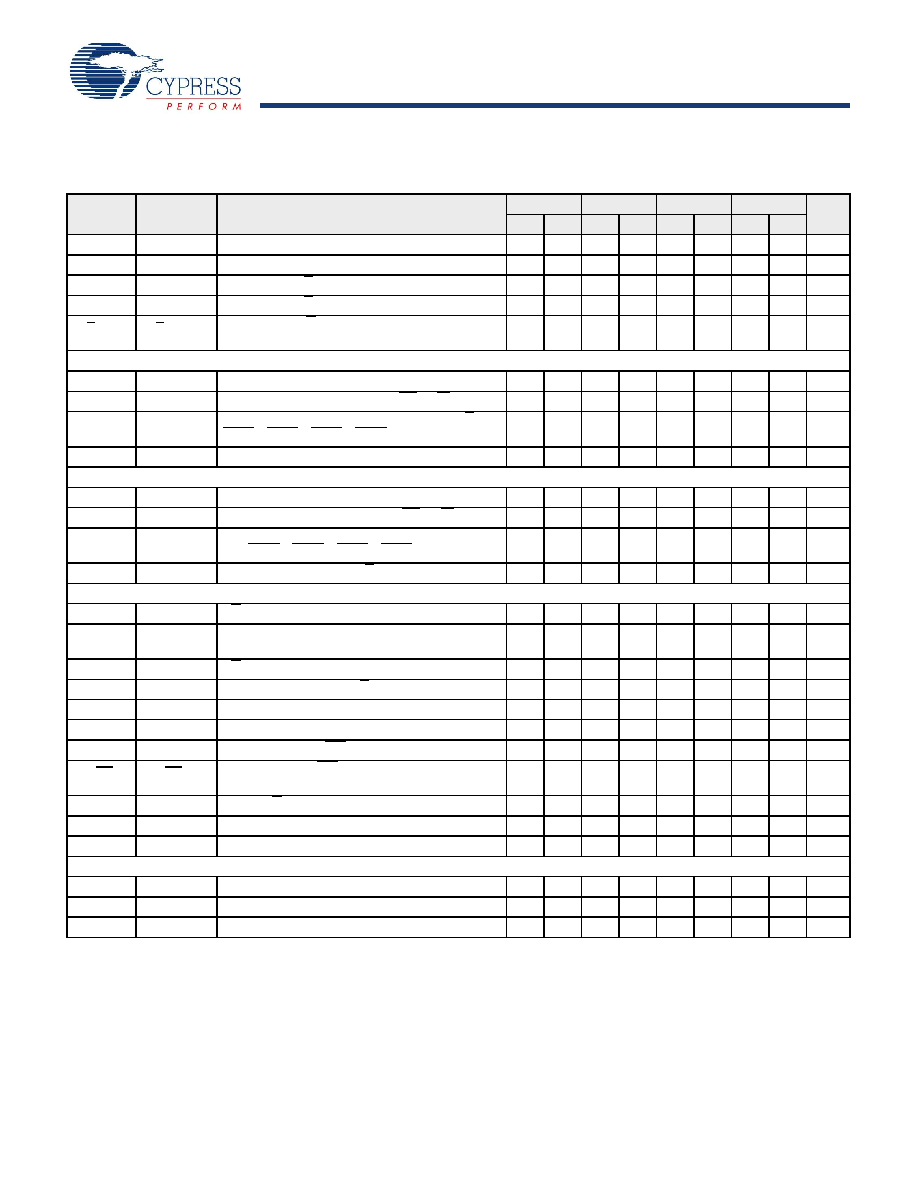
Switching Characteristics
Over the Operating Range [27, 28]
Cypress
Parameter
Consortium
Parameter
Description
450 MHz
400 MHz
375 MHz
333 MHz
Unit
Min Max Min Max Min Max Min Max
tPOWER
1–
1
–
1
–
1–
ms
tCYC
tKHKH
K clock cycle time
2.20 8.4 2.50 8.4 2.66
8.4
3.0
8.4
ns
tKH
tKHKL
Input clock (K/K) HIGH
0.4–0.4
–0.4–0.4
–
ns
tKL
tKLKH
Input clock (K/K) LOW
0.4–0.4
–0.4–0.4
–
ns
tKHKH
K clock rise to K clock rise
(rising edge to rising edge)
0.94
–1.06–
1.13–1.28
–
ns
Setup Times
tSA
tAVKH
Address set-up to K clock rise
0.275
–
0.4
–
0.4
–
0.4
–
ns
tSC
tIVKH
Control set-up to K clock rise (LD, R/W)
0.275
–0.4
–0.4–0.4
–
ns
tSCDDR
tIVKH
Double data rate control set-up to clock (K/K) rise
(BWS0, BWS1, BWS2, BWS3)
0.22
–0.28–
0.28–0.28
–
ns
tSD
tDVKH
D[X:0] set-up to clock (K/K) rise
0.22
–0.28–
0.28–0.28
–
ns
Hold Times
tHA
tKHAX
Address hold after K clock rise
0.275
–
0.4
–
0.4
–
0.4
–
ns
tHC
tKHIX
Control hold after K clock rise (LD, R/W)
0.275
–0.4
–0.4–0.4
–
ns
tHCDDR
tKHIX
Double data rate control hold after clock (K/K)
rise (BWS0, BWS1, BWS2, BWS3)
0.22
–0.28–
0.28–0.28
–
ns
tHD
tKHDX
D[X:0] hold after clock (K/K) rise
0.22
–0.28–
0.28–0.28
–
ns
Output Times
tCO
tCHQV
K/K clock rise to data valid
–
0.45
–
0.45
–
0.45
–
0.45
ns
tDOH
tCHQX
Data output hold after output K/K clock rise
(active to active)
–0.45
–
–0.45
–
–0.45
–
–0.45
–
ns
tCCQO
tCHCQV
K/K clock rise to echo clock valid
–
0.45–
0.45
–0.45–
0.45
ns
tCQOH
tCHCQX
Echo clock hold after K/K clock rise
–0.45
–
–0.45
–
–0.45
–
–0.45
–
ns
tCQD
tCQHQV
Echo clock high to data valid
–
0.15
–
0.20
–
0.20
–
0.20
ns
tCQDOH
tCQHQX
Echo clock high to data invalid
–0.15
–
–0.20
–
–0.20
–
–0.20
–
ns
tCQH
tCQHCQL
Output clock (CQ/CQ) HIGH [30]
0.85
–1.00–
1.08–1.25
–
ns
tCQHCQH tCQHCQH
CQ clock rise to CQ clock rise
(rising edge to rising edge) [30]
0.85
–1.00–
1.08–1.25
–
ns
tCHZ
tCHQZ
Clock (K/K) rise to high Z (active to high Z) [31, 32]
–
0.45–
0.45
–0.45–
0.45
ns
tCLZ
tCHQX1
Clock (K/K) rise to low Z [31, 32]
–0.45
–
–0.45
–
–0.45
–
–0.45
–
ns
tQVLD
tCQHQVLD
Echo clock high to QVLD valid [33]
–0.15 0.15 –0.20 0.20 –0.20 0.20 –0.20 0.20
ns
PLL Timing
tKC Var
Clock phase jitter
–
0.15
–
0.20
–
0.20
–
0.20
ns
tKC lock
PLL lock time (K)
20–20–20–20–
s
tKC Reset
K static to PLL reset [34]
30–30–30–30–
ns
Notes
27. Unless otherwise noted, test conditions assume signal transition time of 2 V/ns, timing reference levels of 0.75 V, VREF = 0.75 V, RQ = 250 , VDDQ = 1.5 V, input pulse
levels of 0.25 V to 1.25 V, and output loading of the specified IOL/IOH and load capacitance shown in (a) of AC Test Loads and Waveforms.
28. When a part with a maximum frequency above 333 MHz is operating at a lower clock frequency, it requires the input timings of the frequency range in which it is being
operated and outputs data with the output timings of that frequency range.
29. This part has an internal voltage regulator; tPOWER is the time that the power is supplied above VDD min initially before a read or write operation can be initiated.
30. These parameters are extrapolated from the input timing parameters (tCYC/2 - 250 ps, where 250 ps is the internal jitter). These parameters are only guaranteed by
design and are not tested in production.
31. tCHZ, tCLZ are specified with a load capacitance of 5 pF as in (b) of AC Test Loads and Waveforms. Transition is measured 100 mV from steady-state voltage.
32. At any voltage and temperature tCHZ is less than tCLZ and tCHZ less than tCO.
33. tQVLD specification is applicable for both rising and falling edges of QVLD signal.
34. Hold to >VIH or <VIL.
相关PDF资料 |
PDF描述 |
|---|---|
| CY7C1371AV25-66AC | 512K X 36 ZBT SRAM, 10 ns, PQFP100 |
| CY7C1387DV25-225BZI | 1M X 18 CACHE SRAM, 2.8 ns, PBGA165 |
| CY7C1387DV25-225BZC | 1M X 18 CACHE SRAM, 2.8 ns, PBGA165 |
| CY7C138AV | Memory |
| CY7C025-15JC | x16 Dual-Port SRAM |
相关代理商/技术参数 |
参数描述 |
|---|---|
| CY7C1248KV18-450BZXC | 功能描述:静态随机存取存储器 36MB (2Mx18) 1.8v 450MHz DDR II 静态随机存取存储器 RoHS:否 制造商:Cypress Semiconductor 存储容量:16 Mbit 组织:1 M x 16 访问时间:55 ns 电源电压-最大:3.6 V 电源电压-最小:2.2 V 最大工作电流:22 uA 最大工作温度:+ 85 C 最小工作温度:- 40 C 安装风格:SMD/SMT 封装 / 箱体:TSOP-48 封装:Tray |
| CY7C12501KV | 制造商:Rochester Electronics LLC 功能描述: 制造商:Cypress Semiconductor 功能描述: |
| CY7C12501KV18-400BZC | 功能描述:静态随机存取存储器 1Mb x 36 400 MHz Sync 静态随机存取存储器 RoHS:否 制造商:Cypress Semiconductor 存储容量:16 Mbit 组织:1 M x 16 访问时间:55 ns 电源电压-最大:3.6 V 电源电压-最小:2.2 V 最大工作电流:22 uA 最大工作温度:+ 85 C 最小工作温度:- 40 C 安装风格:SMD/SMT 封装 / 箱体:TSOP-48 封装:Tray |
| CY7C12501KV18-400BZXC | 功能描述:静态随机存取存储器 1Mb x 36 400 MHz Sync 静态随机存取存储器 RoHS:否 制造商:Cypress Semiconductor 存储容量:16 Mbit 组织:1 M x 16 访问时间:55 ns 电源电压-最大:3.6 V 电源电压-最小:2.2 V 最大工作电流:22 uA 最大工作温度:+ 85 C 最小工作温度:- 40 C 安装风格:SMD/SMT 封装 / 箱体:TSOP-48 封装:Tray |
| CY7C12501KV18-450BZXC | 功能描述:IC SRAM 36MBIT 450MHZ 165-FPBGA RoHS:是 类别:集成电路 (IC) >> 存储器 系列:- 标准包装:150 系列:- 格式 - 存储器:EEPROMs - 串行 存储器类型:EEPROM 存储容量:4K (2 x 256 x 8) 速度:400kHz 接口:I²C,2 线串口 电源电压:2.5 V ~ 5.5 V 工作温度:-40°C ~ 85°C 封装/外壳:8-VFDFN 裸露焊盘 供应商设备封装:8-DFN(2x3) 包装:管件 产品目录页面:1445 (CN2011-ZH PDF) |
发布紧急采购,3分钟左右您将得到回复。