参数资料
| 型号: | DS33ZH11+ |
| 厂商: | Maxim Integrated Products |
| 文件页数: | 79/172页 |
| 文件大小: | 0K |
| 描述: | IC MAPPER ETHERNET 100CSBGA |
| 产品培训模块: | Lead (SnPb) Finish for COTS Obsolescence Mitigation Program |
| 标准包装: | 7 |
| 应用: | 数据传输 |
| 接口: | 串行 |
| 电源电压: | 1.8V,2.5V,3.3V |
| 封装/外壳: | 100-LFBGA,CSPBGA |
| 供应商设备封装: | 100-CSBGA(10x10) |
| 包装: | 托盘 |
| 安装类型: | 表面贴装 |
第1页第2页第3页第4页第5页第6页第7页第8页第9页第10页第11页第12页第13页第14页第15页第16页第17页第18页第19页第20页第21页第22页第23页第24页第25页第26页第27页第28页第29页第30页第31页第32页第33页第34页第35页第36页第37页第38页第39页第40页第41页第42页第43页第44页第45页第46页第47页第48页第49页第50页第51页第52页第53页第54页第55页第56页第57页第58页第59页第60页第61页第62页第63页第64页第65页第66页第67页第68页第69页第70页第71页第72页第73页第74页第75页第76页第77页第78页当前第79页第80页第81页第82页第83页第84页第85页第86页第87页第88页第89页第90页第91页第92页第93页第94页第95页第96页第97页第98页第99页第100页第101页第102页第103页第104页第105页第106页第107页第108页第109页第110页第111页第112页第113页第114页第115页第116页第117页第118页第119页第120页第121页第122页第123页第124页第125页第126页第127页第128页第129页第130页第131页第132页第133页第134页第135页第136页第137页第138页第139页第140页第141页第142页第143页第144页第145页第146页第147页第148页第149页第150页第151页第152页第153页第154页第155页第156页第157页第158页第159页第160页第161页第162页第163页第164页第165页第166页第167页第168页第169页第170页第171页第172页
DS33Z11 Ethernet Mapper
17 of 172
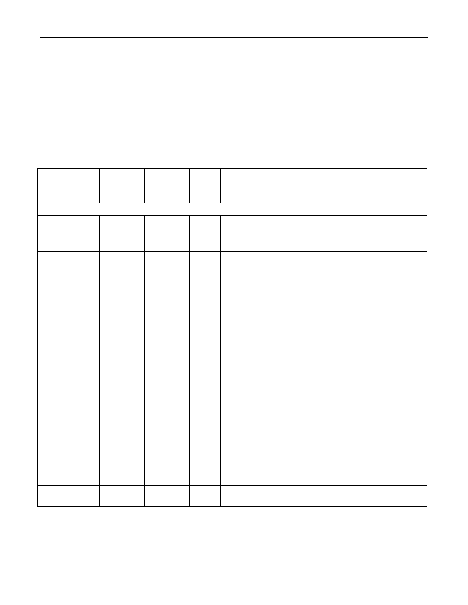
7 PIN DESCRIPTIONS
7.1 Pin Functional Description
Note that all digital pins are IO pins in JTAG mode. This feature increases the effectiveness of board level ATPG
patterns. JTAG pins are not available on the Hardware mode/SPI-only DS33ZH11 (10mm CSBGA)
Note: I = Input; O = Output; Ipu = Input, with pullup; Oz = Output, with tri-state; IO = Bidirectional pin; IOz = Bidirectional pin, with tri-state
Table 7-1 Detailed Pin Descriptions
NAME
PIN #
DS33Z11
CSBGA
(169)
PIN #
DS33ZH1
1
BGA(100)
TYPE
FUNCTION
SERIAL INTERFACE IO PINS
TCLKI
F1
B1
I
Serial Interface Transmit Clock Input: The clock
reference for TSER, which is output on the rising edge of
the clock. TCLKI supports gapped clocking, up to a
maximum frequency of 52 MHz.
TSER
F2
A2
O
Transmit Serial Data Output: Output on the rising edge
of TCLKI. Selective clock periods can be skipped for
output of TSER dependent on the TDEN settings or
gapped clock input (TCLKI). The maximum data rate is 52
Mbps.
TDEN/
TBSYNC
F5
—
IO
Transmit Data Enable (Input): The transmit data enable
is programmable to selectively block/enable the transmit
data. The TDEN signal must occur one clock edge prior to
the affected data bit. The active polarity of TDEN is
programmable in register LI.TSLCR. It is recommended
for both T1/E1 and T3/E3 applications that use gapped
clocks. The TDEN signal is provided for interfacing to
framers that do not have a gapped clock facility.
Transmit Byte Sync (Output): This output can be used
by an external Serial to Parallel to convert TSER stream to
byte wide data. This output indicates the last bit of the
byte data sent serially on TSER. This signal is only active
in the X.86 Mode.
Note that while in Hardware mode with HDLC (non X.86)
operation, this pin must be tied high.
RCLKI
G2
B2
I
Serial Interface Receive Clock Input: Reference clock
for receive serial data on RSER. Gapped clocking is
supported, up to the maximum RCLKI frequency of 52
MHz.
RSER
H1
B3
I
Receive Serial Data Input: Receive Serial data arrives on
the rising edge of the clock.
相关PDF资料 |
PDF描述 |
|---|---|
| DS34C87TN/NOPB | IC LINE DRIVER QUAD CMOS 16-DIP |
| DS34LV87TMX/NOPB | IC LINE DVR QUAD CMOS DIF 16SOIC |
| DS34S132GN+ | IC TDM OVER PACKET 676-BGA |
| DS34T102GN+ | IC TDM OVER PACKET 484TEBGA |
| DS3501U+H | IC POT NV 128POS HV 10-USOP |
相关代理商/技术参数 |
参数描述 |
|---|---|
| DS33ZH11+ | 功能描述:网络控制器与处理器 IC 10/100 ENETXPORT HMODE MAP IND RoHS:否 制造商:Micrel 产品:Controller Area Network (CAN) 收发器数量: 数据速率: 电源电流(最大值):595 mA 最大工作温度:+ 85 C 安装风格:SMD/SMT 封装 / 箱体:PBGA-400 封装:Tray |
| DS34 | 制造商:LUMILEDS 制造商全称:LUMILEDS 功能描述:power light source Luxeon V Emitter |
| DS-3400D UK | 制造商:TRUST 功能描述:DESKTOP WIRELESS OPTICAL TRUST |
| DS3404FP000 | 制造商:Thomas & Betts 功能描述:30A,PLG,3P4W,MG,404,3P480V |
| DS3404FP000/JG63 | 制造商:Thomas & Betts 功能描述:30A,CON,3P4W,MG,404,3P480V,JG63,SC |
发布紧急采购,3分钟左右您将得到回复。