- 您现在的位置:买卖IC网 > PDF目录1917 > DSP56303VL100B1 (Freescale Semiconductor)IC DSP 24BIT 100MHZ 196-BGA PDF资料下载
参数资料
| 型号: | DSP56303VL100B1 |
| 厂商: | Freescale Semiconductor |
| 文件页数: | 22/108页 |
| 文件大小: | 0K |
| 描述: | IC DSP 24BIT 100MHZ 196-BGA |
| 标准包装: | 630 |
| 系列: | DSP563xx |
| 类型: | 定点 |
| 接口: | 主机接口,SSI,SCI |
| 时钟速率: | 100MHz |
| 非易失内存: | ROM(576 B) |
| 芯片上RAM: | 24kB |
| 电压 - 输入/输出: | 3.30V |
| 电压 - 核心: | 3.30V |
| 工作温度: | -40°C ~ 100°C |
| 安装类型: | 表面贴装 |
| 封装/外壳: | 196-LBGA |
| 供应商设备封装: | 196-MAPBGA(15x15) |
| 包装: | 托盘 |
第1页第2页第3页第4页第5页第6页第7页第8页第9页第10页第11页第12页第13页第14页第15页第16页第17页第18页第19页第20页第21页当前第22页第23页第24页第25页第26页第27页第28页第29页第30页第31页第32页第33页第34页第35页第36页第37页第38页第39页第40页第41页第42页第43页第44页第45页第46页第47页第48页第49页第50页第51页第52页第53页第54页第55页第56页第57页第58页第59页第60页第61页第62页第63页第64页第65页第66页第67页第68页第69页第70页第71页第72页第73页第74页第75页第76页第77页第78页第79页第80页第81页第82页第83页第84页第85页第86页第87页第88页第89页第90页第91页第92页第93页第94页第95页第96页第97页第98页第99页第100页第101页第102页第103页第104页第105页第106页第107页第108页
DSP56303 Technical Data, Rev. 11
1-16
Freescale Semiconductor
Signals/Connections
1.12 JTAG and OnCE Interface
The DSP56300 family and in particular the DSP56303 support circuit-board test strategies based on the IEEE
Std. 1149.1 test access port and boundary scan architecture, the industry standard developed under the
sponsorship of the Test Technology Committee of IEEE and the JTAG. The OnCE module provides a means to
interface nonintrusively with the DSP56300 core and its peripherals so that you can examine registers, memory, or
on-chip peripherals. Functions of the OnCE module are provided through the JTAG TAP signals. For programming
models, see the chapter on debugging support in the DSP56300 Family Manual.
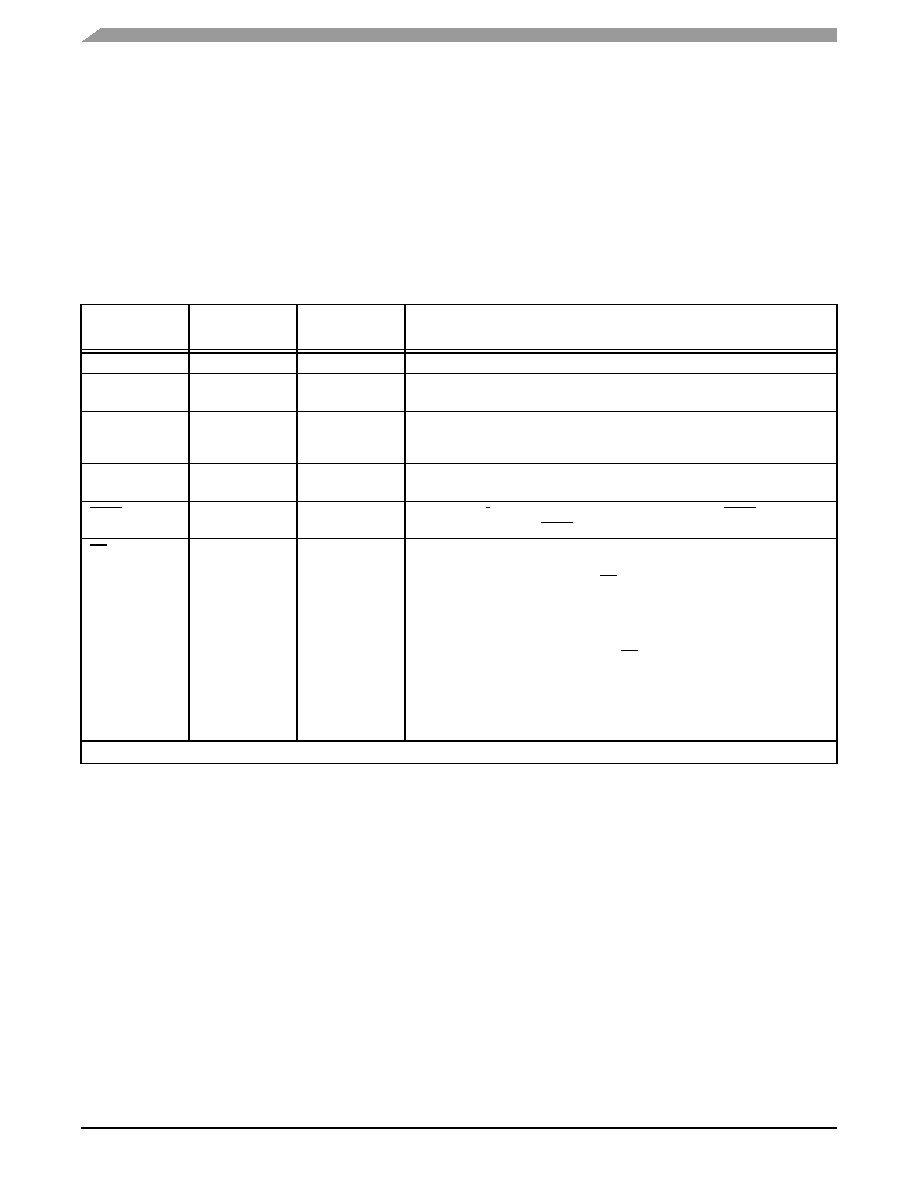
Table 1-16.
JTAG/OnCE Interface
Signal
Name
Type
State During
Reset
Signal Description
TCK
Input
Test Clock—A test clock input signal to synchronize the JTAG test logic.
TDI
Input
Test Data Input—A test data serial input signal for test instructions and data.
TDI is sampled on the rising edge of TCK and has an internal pull-up resistor.
TDO
Output
Tri-stated
Test Data Output—A test data serial output signal for test instructions and
data. TDO is actively driven in the shift-IR and shift-DR controller states. TDO
changes on the falling edge of TCK.
TMS
Input
Test Mode Select—Sequences the test controller’s state machine. TMS is
sampled on the rising edge of TCK and has an internal pull-up resistor.
TRST
Input
Test Reset—Initializes the test controller asynchronously. TRST has an
internal pull-up resistor. TRST must be asserted after powerup.
DE
Input/ Output
(open-drain)
Input
Debug Event—As an input, initiates Debug mode from an external command
controller, and, as an open-drain output, acknowledges that the chip has
entered Debug mode. As an input, DE causes the DSP56300 core to finish
executing the current instruction, save the instruction pipeline information,
enter Debug mode, and wait for commands to be entered from the debug
serial input line. This signal is asserted as an output for three clock cycles
when the chip enters Debug mode as a result of a debug request or as a result
of meeting a breakpoint condition. The DE has an internal pull-up resistor.
This signal is not a standard part of the JTAG TAP controller. The signal
connects directly to the OnCE module to initiate debug mode directly or to
provide a direct external indication that the chip has entered Debug mode. All
other interface with the OnCE module must occur through the JTAG port.
Note: All inputs are 5 V tolerant.
相关PDF资料 |
PDF描述 |
|---|---|
| DSP56311VF150B1 | IC DSP 24BIT 150MHZ 196-BGA |
| DSP56321VF200R2 | IC DSP 24BIT 200MHZ 196-BGA |
| DSP56852VFE | IC DSP 16BIT 120MHZ 81-MAPBGA |
| DSP56854FGE | IC DSP 16BIT 120MHZ 128-LQFP |
| DSP56855BUE | IC DSP 16BIT 120MHZ 100-LQFP |
相关代理商/技术参数 |
参数描述 |
|---|---|
| DSP56304GC66 | 制造商:未知厂家 制造商全称:未知厂家 功能描述:24-Bit Digital Signal Processor |
| DSP56304GC80 | 制造商:未知厂家 制造商全称:未知厂家 功能描述:24-Bit Digital Signal Processor |
| DSP56304PV66 | 制造商:未知厂家 制造商全称:未知厂家 功能描述:24-Bit Digital Signal Processor |
| DSP56304PV80 | 制造商:未知厂家 制造商全称:未知厂家 功能描述:24-Bit Digital Signal Processor |
| DSP56305DS | 制造商:未知厂家 制造商全称:未知厂家 功能描述:DSP56305 Single Chip Channel Codec Digital Signal Processor Data Sheet |
发布紧急采购,3分钟左右您将得到回复。