- 您现在的位置:买卖IC网 > PDF目录1917 > DSP56303VL100B1 (Freescale Semiconductor)IC DSP 24BIT 100MHZ 196-BGA PDF资料下载
参数资料
| 型号: | DSP56303VL100B1 |
| 厂商: | Freescale Semiconductor |
| 文件页数: | 64/108页 |
| 文件大小: | 0K |
| 描述: | IC DSP 24BIT 100MHZ 196-BGA |
| 标准包装: | 630 |
| 系列: | DSP563xx |
| 类型: | 定点 |
| 接口: | 主机接口,SSI,SCI |
| 时钟速率: | 100MHz |
| 非易失内存: | ROM(576 B) |
| 芯片上RAM: | 24kB |
| 电压 - 输入/输出: | 3.30V |
| 电压 - 核心: | 3.30V |
| 工作温度: | -40°C ~ 100°C |
| 安装类型: | 表面贴装 |
| 封装/外壳: | 196-LBGA |
| 供应商设备封装: | 196-MAPBGA(15x15) |
| 包装: | 托盘 |
第1页第2页第3页第4页第5页第6页第7页第8页第9页第10页第11页第12页第13页第14页第15页第16页第17页第18页第19页第20页第21页第22页第23页第24页第25页第26页第27页第28页第29页第30页第31页第32页第33页第34页第35页第36页第37页第38页第39页第40页第41页第42页第43页第44页第45页第46页第47页第48页第49页第50页第51页第52页第53页第54页第55页第56页第57页第58页第59页第60页第61页第62页第63页当前第64页第65页第66页第67页第68页第69页第70页第71页第72页第73页第74页第75页第76页第77页第78页第79页第80页第81页第82页第83页第84页第85页第86页第87页第88页第89页第90页第91页第92页第93页第94页第95页第96页第97页第98页第99页第100页第101页第102页第103页第104页第105页第106页第107页第108页
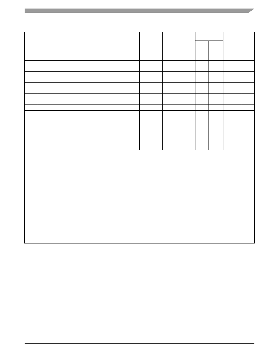
AC Electrical Characteristics
DSP56303 Technical Data, Rev. 11
Freescale Semiconductor
2-39
453
TXC rising edge to transmitter 0 drive enable assertion
—
34.0
20.0
x ck
i ck
ns
454
TXC rising edge to data out valid
—
20.0
8
10.0
x ck
i ck
ns
455
TXC rising edge to data out high impedance
3
—
31.0
16.0
x ck
i ck
ns
456
TXC rising edge to Transmitter 0 drive enable deassertion
3
—
34.0
20.0
x ck
i ck
ns
457
FST input (bl, wr) set-up time before TXC falling edge
2
2.0
21.0
—
x ck
i ck
ns
458
FST input (wl) to data out enable from high impedance
—
27.0
—
ns
459
FST input (wl) to Transmitter 0 drive enable assertion
—
31.0
—
ns
460
FST input (wl) set-up time before TXC falling edge
2.5
21.0
—
x ck
i ck
ns
461
FST input hold time after TXC falling edge
4.0
0.0
—
x ck
i ck
ns
462
Flag output valid after TXC rising edge
—
32.0
18.0
x ck
i ck
ns
Notes:
1.
For the internal clock, the external clock cycle is defined by Icyc (see Timing 7) and the ESSI Control Register.
2.
The word-length-relative frame sync signal waveform operates the same way as the bit-length frame sync signal waveform,
but spreads from one serial clock before the first bit clock (same as the Bit Length Frame Sync signal) until the one before last
bit clock of the first word in the frame.
3.
Periodically sampled and not 100 percent tested
4.
VCC = 3.3 V ± 0.3 V; TJ = 40°C to +100 °C, CL = 50 pF
5.
TXC (SCK Pin) = transmit clock
RXC (SC0 or SCK pin) = receive clock
FST (SC2 pin) = transmit frame sync
FSR (SC1 or SC2 pin) receive frame sync
6.
i ck = internal clock
x ck = external clock
i ck a = internal clock, Asynchronous mode
(asynchronous implies that TXC and RXC are two different clocks)
i ck s = Internal Clock, Synchronous mode
(synchronous implies that TXC and RXC are the same clock)
7.
bl = bit length; wl = word length; wr = word length relative.
8.
If the DSP core writes to the transmit register during the last cycle before causing an underrun error, the delay is 20 ns + (0.5
× T
C).
9.
An expression is used to compute the number listed as the minimum or maximum value as appropriate.
Table 2-18.
ESSI Timings (Continued)
No.
Characteristics4, 5, 7
Symbol
Expression9
100 MHz
Cond-
ition5
Unit
Min
Max
相关PDF资料 |
PDF描述 |
|---|---|
| DSP56311VF150B1 | IC DSP 24BIT 150MHZ 196-BGA |
| DSP56321VF200R2 | IC DSP 24BIT 200MHZ 196-BGA |
| DSP56852VFE | IC DSP 16BIT 120MHZ 81-MAPBGA |
| DSP56854FGE | IC DSP 16BIT 120MHZ 128-LQFP |
| DSP56855BUE | IC DSP 16BIT 120MHZ 100-LQFP |
相关代理商/技术参数 |
参数描述 |
|---|---|
| DSP56304GC66 | 制造商:未知厂家 制造商全称:未知厂家 功能描述:24-Bit Digital Signal Processor |
| DSP56304GC80 | 制造商:未知厂家 制造商全称:未知厂家 功能描述:24-Bit Digital Signal Processor |
| DSP56304PV66 | 制造商:未知厂家 制造商全称:未知厂家 功能描述:24-Bit Digital Signal Processor |
| DSP56304PV80 | 制造商:未知厂家 制造商全称:未知厂家 功能描述:24-Bit Digital Signal Processor |
| DSP56305DS | 制造商:未知厂家 制造商全称:未知厂家 功能描述:DSP56305 Single Chip Channel Codec Digital Signal Processor Data Sheet |
发布紧急采购,3分钟左右您将得到回复。