- 您现在的位置:买卖IC网 > PDF目录1917 > DSP56303VL100B1 (Freescale Semiconductor)IC DSP 24BIT 100MHZ 196-BGA PDF资料下载
参数资料
| 型号: | DSP56303VL100B1 |
| 厂商: | Freescale Semiconductor |
| 文件页数: | 44/108页 |
| 文件大小: | 0K |
| 描述: | IC DSP 24BIT 100MHZ 196-BGA |
| 标准包装: | 630 |
| 系列: | DSP563xx |
| 类型: | 定点 |
| 接口: | 主机接口,SSI,SCI |
| 时钟速率: | 100MHz |
| 非易失内存: | ROM(576 B) |
| 芯片上RAM: | 24kB |
| 电压 - 输入/输出: | 3.30V |
| 电压 - 核心: | 3.30V |
| 工作温度: | -40°C ~ 100°C |
| 安装类型: | 表面贴装 |
| 封装/外壳: | 196-LBGA |
| 供应商设备封装: | 196-MAPBGA(15x15) |
| 包装: | 托盘 |
第1页第2页第3页第4页第5页第6页第7页第8页第9页第10页第11页第12页第13页第14页第15页第16页第17页第18页第19页第20页第21页第22页第23页第24页第25页第26页第27页第28页第29页第30页第31页第32页第33页第34页第35页第36页第37页第38页第39页第40页第41页第42页第43页当前第44页第45页第46页第47页第48页第49页第50页第51页第52页第53页第54页第55页第56页第57页第58页第59页第60页第61页第62页第63页第64页第65页第66页第67页第68页第69页第70页第71页第72页第73页第74页第75页第76页第77页第78页第79页第80页第81页第82页第83页第84页第85页第86页第87页第88页第89页第90页第91页第92页第93页第94页第95页第96页第97页第98页第99页第100页第101页第102页第103页第104页第105页第106页第107页第108页
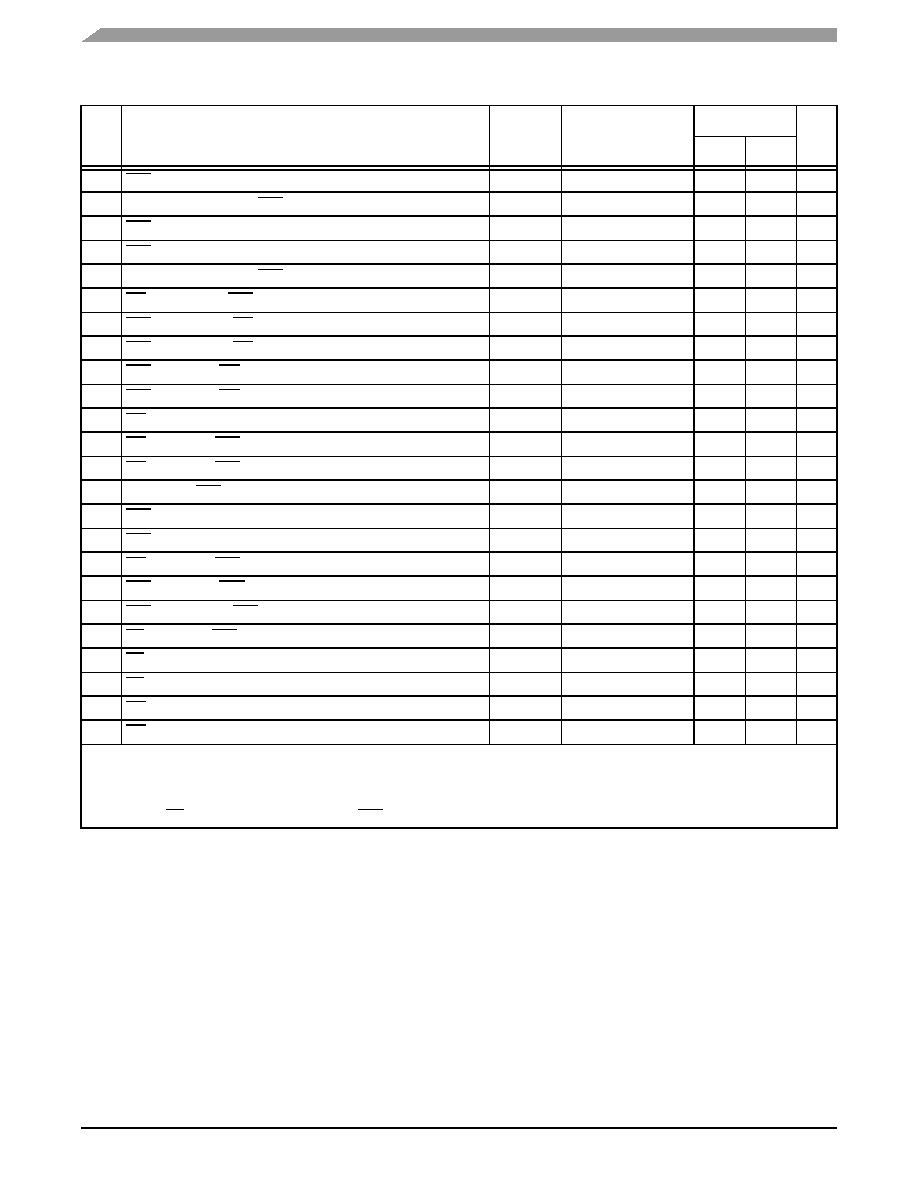
DSP56303 Technical Data, Rev. 11
2-20
Freescale Semiconductor
Specifications
172
RAS assertion to row address not valid
tRAH
1.75
× TC 4.0
13.5
—
ns
173
Column address valid to CAS assertion
tASC
0.75
× T
C 4.0
3.5
—
ns
174
CAS assertion to column address not valid
tCAH
5.25
× TC 4.0
48.5
—
ns
175
RAS assertion to column address not valid
tAR
7.75
× TC 4.0
73.5
—
ns
176
Column address valid to RAS deassertion
tRAL
6
× T
C 4.0
56.0
—
ns
177
WR deassertion to CAS assertion
tRCS
3.0
× TC 4.0
26.0
—
ns
178
CAS deassertion to WR
4 assertion
tRCH
1.75
× TC – 3.7
13.8
—
ns
179
RAS deassertion to WR4 assertion
tRRH
0.25
× T
C 2.0
0.5
—
ns
180
CAS assertion to WR deassertion
tWCH
5
× TC 4.2
45.8
—
ns
181
RAS assertion to WR deassertion
tWCR
7.5
× TC 4.2
70.8
—
ns
182
WR assertion pulse width
tWP
11.5
× T
C 4.5
110.5
—
ns
183
WR assertion to RAS deassertion
tRWL
11.75
× TC 4.3
113.2
—
ns
184
WR assertion to CAS deassertion
tCWL
10.25
× TC 4.3
98.2
—
ns
185
Data valid to CAS assertion (write)
tDS
5.75
× T
C 4.0
53.5
—
ns
186
CAS assertion to data not valid (write)
tDH
5.25
× TC 4.0
48.5
—
ns
187
RAS assertion to data not valid (write)
tDHR
7.75
× TC 4.0
73.5
—
ns
188
WR assertion to CAS assertion
tWCS
6.5
× T
C 4.3
60.7
—
ns
189
CAS assertion to RAS assertion (refresh)
tCSR
1.5
× TC 4.0
11.0
—
ns
190
RAS deassertion to CAS assertion (refresh)
tRPC
2.75
× TC 4.0
23.5
—
ns
191
RD assertion to RAS deassertion
tROH
11.5
× T
C 4.0
111.0
—
ns
192
RD assertion to data valid
tGA
10
× TC 7.0
—
93.0
ns
193
RD deassertion to data not valid
5
tGZ
0.0
—
ns
194
WR assertion to data active
0.75
× T
C – 1.5
6.0
—
ns
195
WR deassertion to data high impedance
0.25
× TC
—2.5
ns
Notes:
1.
The number of wait states for an out-of-page access is specified in the DRAM Control Register.
2.
The refresh period is specified in the DRAM Control Register.
3.
Use the expression to compute the maximum or minimum value listed (or both if the expression includes
±) .
4.
Either tRCH or tRRH must be satisfied for read cycles.
5.
RD deassertion always occurs after CAS deassertion; therefore, the restricted timing is tOFF and not tGZ.
Table 2-11.
DRAM Out-of-Page and Refresh Timings, Eleven Wait States1,2 (Continued)
No.
Characteristics
Symbol
Expression3
100 MHz
Unit
Min
Max
相关PDF资料 |
PDF描述 |
|---|---|
| DSP56311VF150B1 | IC DSP 24BIT 150MHZ 196-BGA |
| DSP56321VF200R2 | IC DSP 24BIT 200MHZ 196-BGA |
| DSP56852VFE | IC DSP 16BIT 120MHZ 81-MAPBGA |
| DSP56854FGE | IC DSP 16BIT 120MHZ 128-LQFP |
| DSP56855BUE | IC DSP 16BIT 120MHZ 100-LQFP |
相关代理商/技术参数 |
参数描述 |
|---|---|
| DSP56304GC66 | 制造商:未知厂家 制造商全称:未知厂家 功能描述:24-Bit Digital Signal Processor |
| DSP56304GC80 | 制造商:未知厂家 制造商全称:未知厂家 功能描述:24-Bit Digital Signal Processor |
| DSP56304PV66 | 制造商:未知厂家 制造商全称:未知厂家 功能描述:24-Bit Digital Signal Processor |
| DSP56304PV80 | 制造商:未知厂家 制造商全称:未知厂家 功能描述:24-Bit Digital Signal Processor |
| DSP56305DS | 制造商:未知厂家 制造商全称:未知厂家 功能描述:DSP56305 Single Chip Channel Codec Digital Signal Processor Data Sheet |
发布紧急采购,3分钟左右您将得到回复。