- 您现在的位置:买卖IC网 > PDF目录295865 > E28F200B5B60 (INTEL CORP) DIRECTIONAL COUPLER, 20DB, SMT PDF资料下载
参数资料
| 型号: | E28F200B5B60 |
| 厂商: | INTEL CORP |
| 元件分类: | PROM |
| 英文描述: | DIRECTIONAL COUPLER, 20DB, SMT |
| 中文描述: | 256K X 8 FLASH 5V PROM, 70 ns, PDSO48 |
| 封装: | 12 X 20 MM, TSOP-48 |
| 文件页数: | 2/44页 |
| 文件大小: | 345K |
| 代理商: | E28F200B5B60 |
第1页当前第2页第3页第4页第5页第6页第7页第8页第9页第10页第11页第12页第13页第14页第15页第16页第17页第18页第19页第20页第21页第22页第23页第24页第25页第26页第27页第28页第29页第30页第31页第32页第33页第34页第35页第36页第37页第38页第39页第40页第41页第42页第43页第44页
28F200B5, 28F004/400B5, 28F800B5
E
10
PRELIMINARY
28F004B5
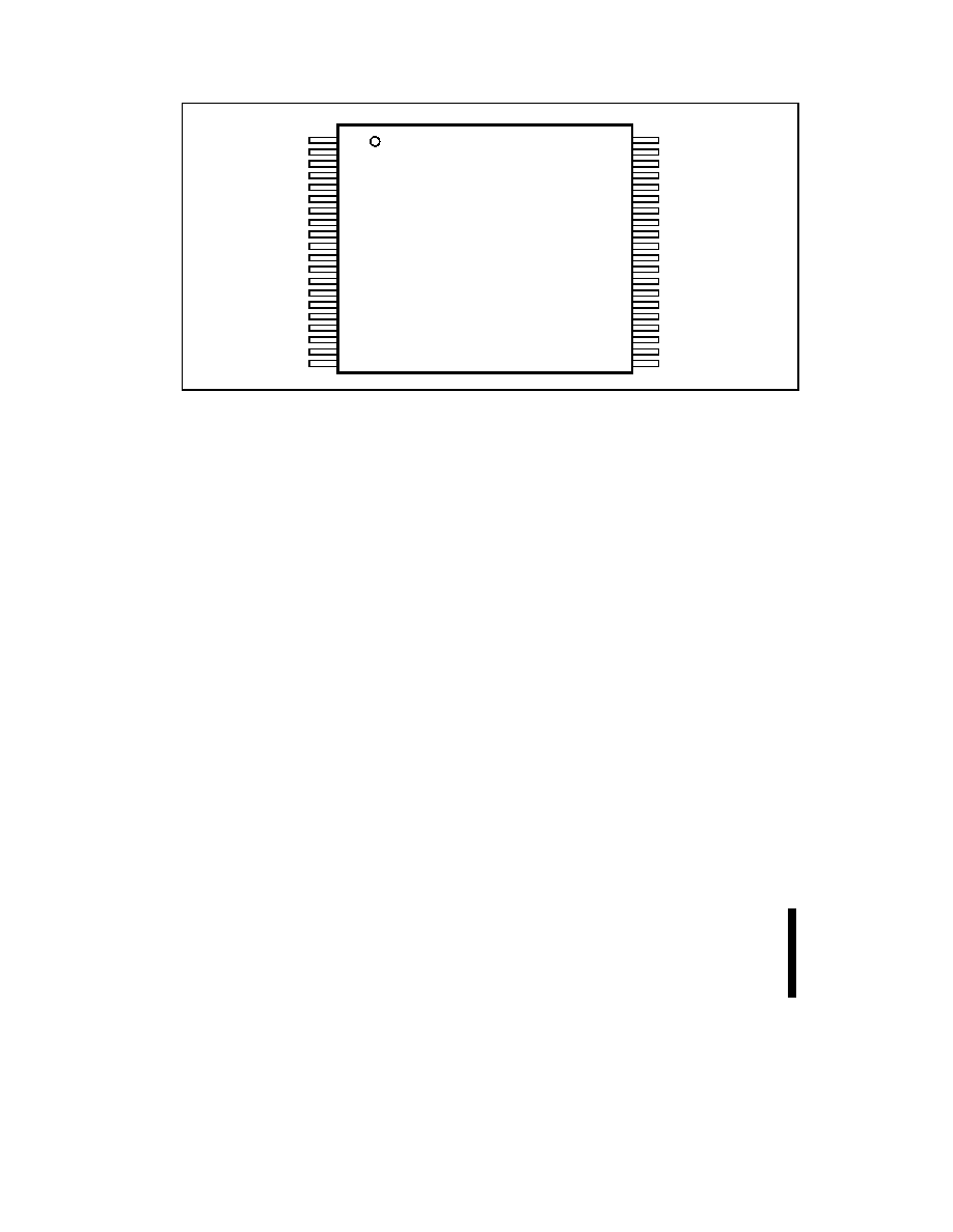
Boot Block
40-Lead TSOP
10 mm x20mm
TOP VIEW
32
31
30
29
28
27
26
25
24
23
22
21
33
34
35
36
37
38
39
40
20
19
17
18
1
2
3
4
5
6
7
8
9
10
11
12
13
14
16
15
A 1
A 2
A 3
RP#
WE#
VPP
A16
A15
A7
A6
A5
A4
A14
A13
A8
A9
A11
A12
WP#
DQ7
CE#
OE#
GND
A0
DQ6
DQ5
DQ4
DQ2
DQ1
DQ0
VCC
DQ3
A17
GND
NC
A10
NC
A18
VCC
Figure 3. 40-Lead TSOP Pinout Diagram (Available in 4-Mbit Only)
2.3
Memory Blocking Organization
The
boot
block
product
family
features
an
asymmetrically-blocked
architecture
providing
system memory integration. Each erase block can
be erased independently of the others up to
100,000 times for commercial temperature or up to
10,000
times
for
extended
temperature.
At
automotive temperature, each parameter block can
be erased independently 30,000 times, and each
main and boot block 1,000 times. The block sizes
have been chosen to optimize their functionality for
common applications of nonvolatile storage. The
combination of block sizes in the boot block
architecture
allow
the
integration
of
several
memories into a single chip. For the address
locations of the blocks, see the memory maps in
Figures 4, 5, 6 and 7.
2.3.1
ONE 16-KB BOOT BLOCK
The boot block is intended to replace a dedicated
boot PROM in a microprocessor or microcontroller-
based system. The 16-Kbyte (16,384 bytes) boot
block is located at either the top (denoted by -T
suffix) or the bottom (-B suffix) of the address map
to accommodate different microprocessor protocols
for boot code location. This boot block features
hardware controllable write-protection to protect the
crucial microprocessor boot code from accidental
modification. The protection of the boot block is
controlled using a combination of the VPP, RP#, and
WP# pins, as is detailed in Section 3.3.
2.3.2
TWO 8-KB PARAMETER BLOCKS
Each boot block component contains two parameter
blocks of 8 Kbytes (8,192 bytes) each to facilitate
storage of frequently updated small parameters that
would normally require an EEPROM. By using
software techniques, the byte-rewrite functionality
of EEPROMs can be emulated. These techniques
are detailed in Intel’s application note,
AP-604
Using Intel’s Boot Block Flash Memory Parameter
Blocks to Replace EEPROM. The parameter blocks
are not write-protectable.
2.3.3
MAIN BLOCKS - ONE 96-KB +
ADDITIONAL 128-KB BLOCKS
After the allocation of address space to the boot
and parameter blocks, the remainder is divided into
main blocks for data or code storage. Each device
contains one 96-Kbyte (98,304 byte) block and
additional 128-Kbyte (131,072 byte) blocks. The
2-Mbit has one 128-KB block; the 4-Mbit, three; and
the 8-Mbit, seven.
相关PDF资料 |
PDF描述 |
|---|---|
| E28F200BX-B120 | 2-MBIT (128K x 16, 256K x 8) BOOT BLOCK FLASH MEMORY FAMILY |
| E28F200BX-B60 | 2-MBIT (128K x 16, 256K x 8) BOOT BLOCK FLASH MEMORY FAMILY |
| E28F200BX-B80 | 2-MBIT (128K x 16, 256K x 8) BOOT BLOCK FLASH MEMORY FAMILY |
| E28F200BX-T120 | 2-MBIT (128K x 16, 256K x 8) BOOT BLOCK FLASH MEMORY FAMILY |
| E28F002BX-T120 | 2-MBIT (128K x 16, 256K x 8) BOOT BLOCK FLASH MEMORY FAMILY |
相关代理商/技术参数 |
参数描述 |
|---|---|
| E28F200B5B80 | 制造商:INTEL 制造商全称:Intel Corporation 功能描述:SMART 5 BOOT BLOCK FLASH MEMORY FAMILY 2, 4, 8 MBIT |
| E28F200B5T60 | 制造商:INTEL 制造商全称:Intel Corporation 功能描述:SMART 5 BOOT BLOCK FLASH MEMORY FAMILY 2, 4, 8 MBIT |
| E28F200B5T80 | 制造商:Rochester Electronics LLC 功能描述:- Bulk 制造商:Intel 功能描述: |
| E28F200BL-B150 | 制造商:INTEL 制造商全称:Intel Corporation 功能描述:2-MBIT (128K x 16, 256K x 8)LOW-POWER BOOT BLOCK FLASH MEMORY FAMILY |
| E28F200BL-T150 | 制造商:INTEL 制造商全称:Intel Corporation 功能描述:2-MBIT (128K x 16, 256K x 8)LOW-POWER BOOT BLOCK FLASH MEMORY FAMILY |
发布紧急采购,3分钟左右您将得到回复。