- 您现在的位置:买卖IC网 > PDF目录295865 > E28F200B5B60 (INTEL CORP) DIRECTIONAL COUPLER, 20DB, SMT PDF资料下载
参数资料
| 型号: | E28F200B5B60 |
| 厂商: | INTEL CORP |
| 元件分类: | PROM |
| 英文描述: | DIRECTIONAL COUPLER, 20DB, SMT |
| 中文描述: | 256K X 8 FLASH 5V PROM, 70 ns, PDSO48 |
| 封装: | 12 X 20 MM, TSOP-48 |
| 文件页数: | 42/44页 |
| 文件大小: | 345K |
| 代理商: | E28F200B5B60 |
第1页第2页第3页第4页第5页第6页第7页第8页第9页第10页第11页第12页第13页第14页第15页第16页第17页第18页第19页第20页第21页第22页第23页第24页第25页第26页第27页第28页第29页第30页第31页第32页第33页第34页第35页第36页第37页第38页第39页第40页第41页当前第42页第43页第44页
E
28F200B5, 28F004/400B5, 28F800B5
7
PRELIMINARY
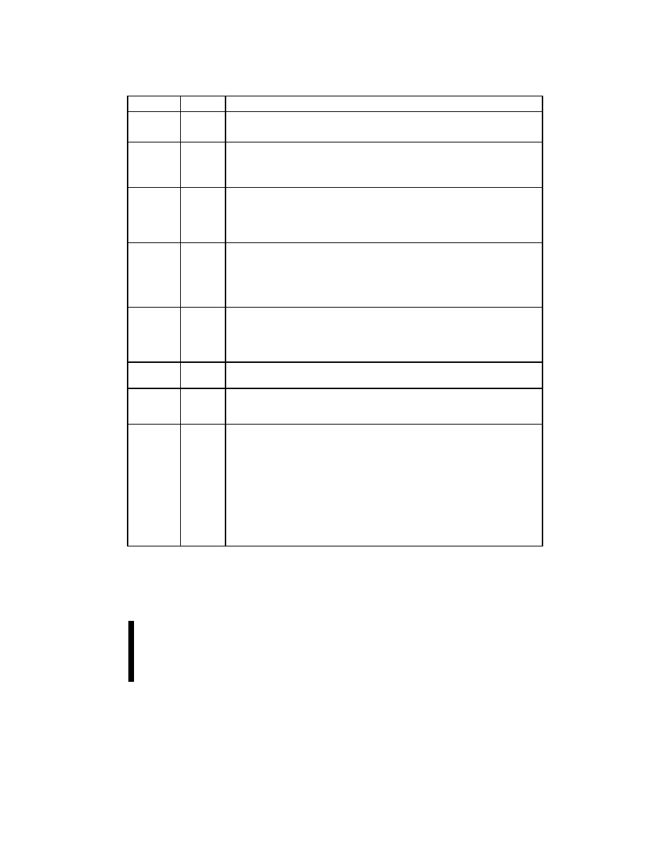
Table 2. Pin Descriptions
Symbol
Type
Name and Function
A0–A18
INPUT
ADDRESS INPUTS for memory addresses. Addresses are internally latched
during a write cycle.
28F200: A[0–16], 28F400: A[0–17], 28F800: A[0–18], 28F004: A[0–18]
A9
INPUT
ADDRESS INPUT: When A9 is at VHH the signature mode is accessed. During
this mode, A0 decodes between the manufacturer and device IDs. When BYTE#
is at a logic low, only the lower byte of the signatures are read. DQ15/A–1 is a
don’t care in the signature mode when BYTE# is low.
DQ0–DQ7
INPUT/
OUTPUT
DATA INPUTS/OUTPUTS: Inputs array data on the second CE# and WE# cycle
during a Program command. Inputs commands to the Command User Interface
when CE# and WE# are active. Data is internally latched during the write cycle.
Outputs array, intelligent identifier and status register data. The data pins float to
tri-state when the chip is de-selected or the outputs are disabled.
DQ8–DQ15
INPUT/
OUTPUT
DATA INPUTS/OUTPUTS: Inputs array data on the second CE# and WE# cycle
during a Program command. Data is internally latched during the write cycle.
Outputs array data. The data pins float to tri-state when the chip is de-selected or
the outputs are disabled as in the byte-wide mode (BYTE# = “0”). In the byte-wide
mode DQ15/A–1 becomes the lowest order address for data output on DQ0–DQ7.
Not applicable to 28F004B5.
CE#
INPUT
CHIP ENABLE: Activates the device’s control logic, input buffers, decoders and
sense amplifiers. CE# is active low. CE# high de-selects the memory device and
reduces power consumption to standby levels. If CE# and RP# are high, but not
at a CMOS high level, the standby current will increase due to current flow
through the CE# and RP# input stages.
OE#
INPUT
OUTPUT ENABLE: Enables the device’s outputs through the data buffers during
a read cycle. OE# is active low.
WE#
INPUT
WRITE ENABLE: Controls writes to the command register and array blocks. WE#
is active low. Addresses and data are latched on the rising edge of the WE#
pulse.
RP#
INPUT
RESET/DEEP POWER-DOWN: Uses three voltage levels (VIL, VIH, and VHH) to
control two different functions: reset/deep power-down mode and boot block
unlocking. It is backwards-compatible with the BX/BL/BV products.
When RP# is at logic low, the device is in reset/deep power-down mode,
which puts the outputs at High-Z, resets the Write State Machine, and draws
minimum current.
When RP# is at logic high, the device is in standard operation. When RP#
transitions from logic-low to logic-high, the device defaults to the read array mode.
When RP# is at VHH, the boot block is unlocked and can be programmed or
erased. This overrides any control from the WP# input.
相关PDF资料 |
PDF描述 |
|---|---|
| E28F200BX-B120 | 2-MBIT (128K x 16, 256K x 8) BOOT BLOCK FLASH MEMORY FAMILY |
| E28F200BX-B60 | 2-MBIT (128K x 16, 256K x 8) BOOT BLOCK FLASH MEMORY FAMILY |
| E28F200BX-B80 | 2-MBIT (128K x 16, 256K x 8) BOOT BLOCK FLASH MEMORY FAMILY |
| E28F200BX-T120 | 2-MBIT (128K x 16, 256K x 8) BOOT BLOCK FLASH MEMORY FAMILY |
| E28F002BX-T120 | 2-MBIT (128K x 16, 256K x 8) BOOT BLOCK FLASH MEMORY FAMILY |
相关代理商/技术参数 |
参数描述 |
|---|---|
| E28F200B5B80 | 制造商:INTEL 制造商全称:Intel Corporation 功能描述:SMART 5 BOOT BLOCK FLASH MEMORY FAMILY 2, 4, 8 MBIT |
| E28F200B5T60 | 制造商:INTEL 制造商全称:Intel Corporation 功能描述:SMART 5 BOOT BLOCK FLASH MEMORY FAMILY 2, 4, 8 MBIT |
| E28F200B5T80 | 制造商:Rochester Electronics LLC 功能描述:- Bulk 制造商:Intel 功能描述: |
| E28F200BL-B150 | 制造商:INTEL 制造商全称:Intel Corporation 功能描述:2-MBIT (128K x 16, 256K x 8)LOW-POWER BOOT BLOCK FLASH MEMORY FAMILY |
| E28F200BL-T150 | 制造商:INTEL 制造商全称:Intel Corporation 功能描述:2-MBIT (128K x 16, 256K x 8)LOW-POWER BOOT BLOCK FLASH MEMORY FAMILY |
发布紧急采购,3分钟左右您将得到回复。