参数资料
| 型号: | HI7188IN |
| 厂商: | Intersil |
| 文件页数: | 13/24页 |
| 文件大小: | 0K |
| 描述: | CONV A/D 16BIT 8:1 MUX 44-MQFP |
| 标准包装: | 96 |
| 位数: | 16 |
| 采样率(每秒): | 240 |
| 数据接口: | QSPI?,串行,SPI? |
| 转换器数目: | 1 |
| 功率耗散(最大): | 50mW |
| 电压电源: | 模拟和数字,双 ± |
| 工作温度: | -40°C ~ 85°C |
| 安装类型: | 表面贴装 |
| 封装/外壳: | 44-QFP |
| 供应商设备封装: | 44-MQFP(10x10) |
| 包装: | 管件 |
| 输入数目和类型: | 8 个差分,单极;8 个差分,双极 |
20
Control Register
The Control Register (CR) is 16 bits wide and contains
information that determines operating mode and the
system/chip level conguration. This conguration applies to
all logical channels and cannot be modied at the channel
level. Following are the bit assignments:
T3, T2, T1 - Bits 15, 14 and 13 are reserved and MUST
always be logic zero for normal operation. These bits are low
after RESET is applied.
CHOP. Bit 12 is the active low chop bit used to determine
whether the chopper stabilized amplier is used or
bypassed. This bit is low (chop on) after RESET is applied.
SE. Bit 11 is the active high suppress EOS bit. If high, the
EOS interrupt will not go active when any logical channel is
in calibration mode. If this bit is high and no logical channels
are in the calibration mode, or this bit is low, EOS
functionality is as previously described. This bit allows the
user to suppress false EOS interrupts during calibration.
Only logical channels that are actively being converted are
considered. That is, if only two logical channels are being
converted but the CCR byte for a non active logical channel
is in a calibration mode, the EOS functionality is active. This
bit is low (suppress EOS off) after RESET is applied.
LNR. Bit 10 is the active high line noise rejection (LNR) bit. If
high LNR is selected. This bit is low (LNR off) after RESET is
applied.
FS. Bit 9 is the 50Hz/60Hz frequency select bit. If bit 9 is
high, the clock generation logic synchronizes conversions for
proper rejection of 50Hz line noise. If bit 9 is low, the clock
generation logic synchronizes conversions for proper
rejection of 60Hz line noise. This bit is low (60Hz LNR) after
RESET is applied.
TC. Bit 8 is the active high two’s complement bit used to
select between 2’s complementary and offset binary data
coding for bipolar mode. In bipolar mode, a high selects
two’s complement; when low data is offset binary. Note that
in unipolar mode the binary data coding is not affected by
the TC bit. This bit is low (offset binary data) after RESET is
applied.
N2, N1, N0. Bits 7, 6 and 5 are the bits that specify the number
of active logical channels to be converted. See Table 8. These
bits are low (one active channel) after RESET is applied.
TP - Bit 4 is the active high two point calibration bit. When
high, the positive gain slope factor is used for both positive
and negative voltages. This bit is low (normal three point cal)
after RESET is applied.
SLP - Bit 3 is the active high sleep mode bit used to put the
device in a low power/standby mode. When high, conversion
stops and the conversion pointer is reset to logical channel
1. The four line noise rejection lters are cleared and EOS is
deactivated. The serial interface, calibration/data RAMs, CR
and CCR are not affected.
To return from sleep mode the user changes this bit from
high to low. This restarts the conversion process beginning
with logical channel 1. If line noise rejection is enabled, it
takes four complete scans (all active channels) to rell the
four line noise rejection lters before an EOS interrupt. If line
noise rejection not enabled, it takes 1 complete scan before
an EOS interrupt.
This bit is low (sleep mode off) after RESET is applied.
BD. Bit 2 is the byte direction bit used to determine either
ascending or descending order access for multi-byte
transfers. When high, ascending order is enabled. When low,
descending order is enabled. This bit is low (descending
order) after RESET is applied.
MSB. Bit 1 bit direction bit used to select whether a serial
data transfer is MSB or LSB rst. When low, MSB rst mode
is enabled while high selects LSB rst. This bit is low (MSB
rst) after RESET is applied.
SDL. Bit 0 selects a two-wire or three-wire transfer protocol of
the serial interface. When low, two-wire data transfers are done
using the SDIO pin. Both data in and out of the part is uses the
by-directional SDIO pin. When high, three-wire data transfers
are done using the SDIO and SDO pins. Data into the part uses
the SDIO pin while data out uses the SDO pin. This bit is low
(two-wire, SDIO exclusively) after RESET is applied.
Channel Conguration Registers
The HI7188 Channel Configuration Registers (CCR) comprise
a 64-bit memory element that defines the logical channel
conversion order as well as each logical channel specific data
such as physical channel address, mode, gain, and
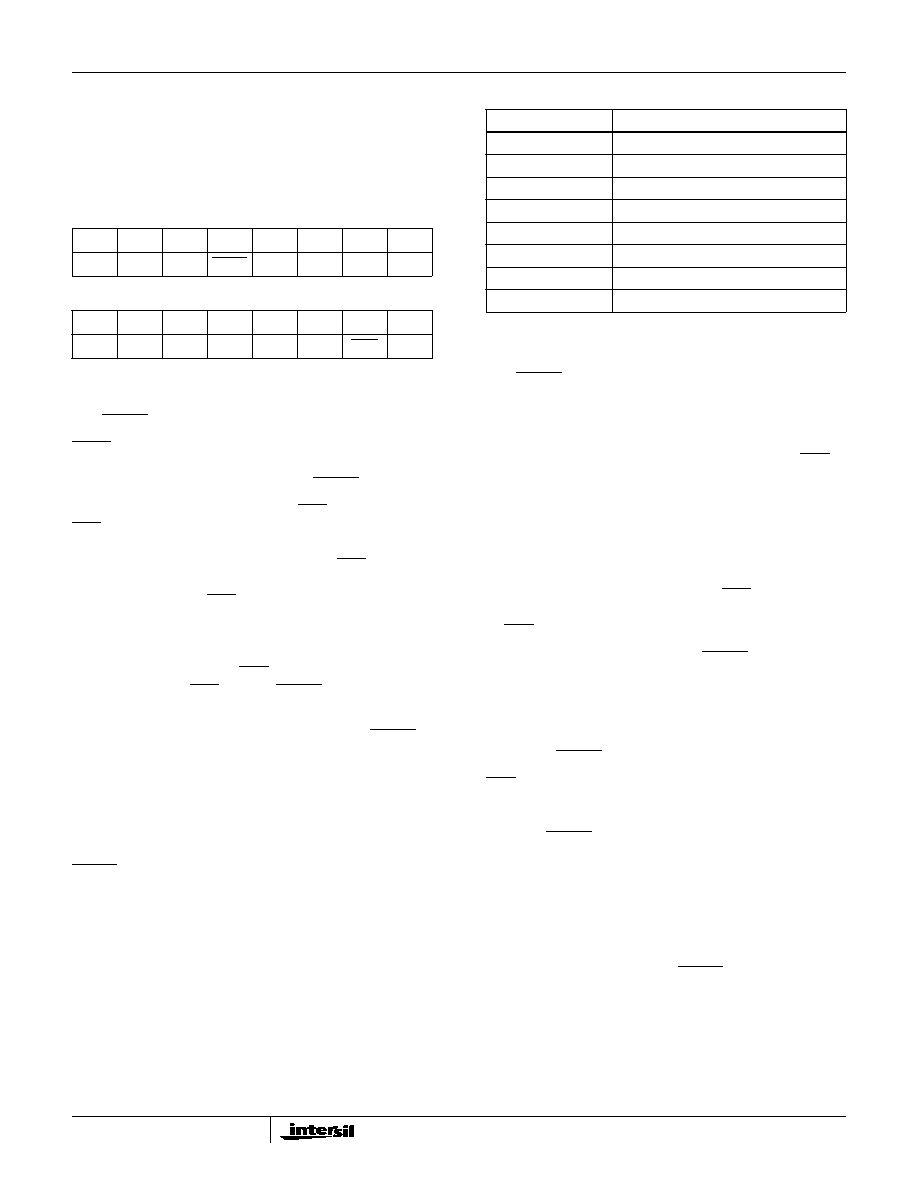
CONTROL REGISTER BYTE 1
MSB
14
13
12
11
10
9
LSB
T3
T2
T1
CHOP
SE
LNR
FS
TC
CONTROL REGISTER BYTE 0
MSB
654321
LSB
N2
N1
N0
TP
SLP
BD
MSB
SDL
TABLE 8. NUMBER OF CONVERSION CHANNELS
N2, N1, N0 CR [7:5]
NUMBER OF CHANNELS TO CONVERT
000
1
001
2
010
3
011
4
100
5
101
6
110
7
111
8
HI7188
相关PDF资料 |
PDF描述 |
|---|---|
| HI7190IP | IC ADC 24BIT PROGBL SER 20-PDIP |
| HI7191IP | IC ADC 24BIT PROGBL SER 20-PDIP |
| HI9P5701K-5 | CONV A/D 6BIT 30MSPS 18-SOIC |
| HMC700LP4E | IC FRACT-N PLL 16BIT 24QFN |
| HMC703LP4E | IC FRACT-N PLL W/SWEEPR 24QFN |
相关代理商/技术参数 |
参数描述 |
|---|---|
| HI7188IP | 制造商:Rochester Electronics LLC 功能描述:- Bulk 制造商:Analog Devices 功能描述:IC 16BIT ADC 7188 DIP40 制造商:Harris Corporation 功能描述: |
| HI7190 | 制造商:INTERSIL 制造商全称:Intersil Corporation 功能描述:null24-Bit, High Precision, Sigma Delta A/D Converter |
| HI7190 WAF | 制造商:Harris Corporation 功能描述: |
| HI7190_06 | 制造商:INTERSIL 制造商全称:Intersil Corporation 功能描述:24-Bit, High Precision, Sigma Delta A/D Converter |
| HI7190EVAL | 功能描述:EVALUATION PLATFORM HI7190 RoHS:否 类别:编程器,开发系统 >> 评估板 - 模数转换器 (ADC) 系列:- 产品培训模块:Obsolescence Mitigation Program 标准包装:1 系列:- ADC 的数量:1 位数:12 采样率(每秒):94.4k 数据接口:USB 输入范围:±VREF/2 在以下条件下的电源(标准):- 工作温度:-40°C ~ 85°C 已用 IC / 零件:MAX11645 已供物品:板,软件 |
发布紧急采购,3分钟左右您将得到回复。