参数资料
| 型号: | HI7188IN |
| 厂商: | Intersil |
| 文件页数: | 2/24页 |
| 文件大小: | 0K |
| 描述: | CONV A/D 16BIT 8:1 MUX 44-MQFP |
| 标准包装: | 96 |
| 位数: | 16 |
| 采样率(每秒): | 240 |
| 数据接口: | QSPI?,串行,SPI? |
| 转换器数目: | 1 |
| 功率耗散(最大): | 50mW |
| 电压电源: | 模拟和数字,双 ± |
| 工作温度: | -40°C ~ 85°C |
| 安装类型: | 表面贴装 |
| 封装/外壳: | 44-QFP |
| 供应商设备封装: | 44-MQFP(10x10) |
| 包装: | 管件 |
| 输入数目和类型: | 8 个差分,单极;8 个差分,双极 |
10
Functional Description
The HI7188 contains a differential 8 channel multiplexer,
Programmable Gain Instrumentation Amplier (PGIA), 4th
order sigma-delta ADC, integrating lter, line noise rejection
lters, Calibration and data RAMs, bidirectional serial port,
clock oscillator, and a microsequencer. The 8 to 1
multiplexer at the input combined with the resetable
modulator on the HI7188 allow for conversions of up to 8
differential channels with each channel being updated at a
rate of 240 samples per second (with 60Hz line noise
rejection enabled). The device can be programmed for
conversion of any combination of physical channels. After
the signal has passed through the multiplexer, it moves into
the PGIA. The PGIA can be congured in gains of 1, 2, 4
and 8 specic for each of the 8 logical channels. The signal
then enters the sigma delta modulator. The patented one-
shot sigma delta modulator is a fourth order modulator which
converts the differential analog signal into a series of one bit
outputs. The 1’s density of this data stream provides a digital
representation of the analog input. The output of the
modulator is fed into the integrating low pass digital lter.
Data out of the lter is available after 201 bits are received
from the modulator.
If the device is in line noise rejection mode, the integrating
lter data is routed to the Line Noise Rejection lters. This
data is then calibrated using the offset and gain calibration
coefcients. Data coding is performed and the result is
stored in the data RAM. If line noise rejection is disabled, the
averaging lter is bypassed, calibration is performed on the
data from the integrating lter, the data is coded, and the
result is stored in the data RAM.
This data ow of modulation, lter and calibrate is repeated
for each of the active logical channels (up to 8). After all
active logical channels are converted the HI7188 generates
an active low interrupt, End Of Scan (EOS), that indicates all
logical channels have been updated and valid data is
available to be read from the data RAM.
Converted data is read via the HI7188 serial I/O port which
is compatible with most synchronous transfer formats
including both the Motorola SPI and Intel 8051 series SSR
protocols. All RAMs, including the Data RAM, are accessed
in a “burst” mode. That is, the data for all active logical
channels is accessed in a single read communication cycle.
Using the HI7188
This section describes how to use the device for a typical
application. This includes power supply considerations, initial
reset, calibration and conversion. Please refer to Figure 7.
The analog and digital supplies and grounds are separate
on the HI7188 to minimize digital noise coupling into the
analog circuitry. Nominal supply voltages are AVDD = +5V,
DVDD = +5V, and AVSS = -5V. If the same supply is used
for AVDD and DVDD it is imperative that the supply is
separately decoupled to the AVDD and DVDD pins on the
HI7188. Separate analog and digital ground planes should
be maintained on the system board and the grounds should
be tied together back at the power supply.
When the HI7188 is powered up it needs to be reset by pulling
the RST line low. This resets the internal registers as shown in
Table 1. This initial configuration defines the part for one
active logical channel (physical channel 1, address 000),
conversion mode, unipolar operation, gain of one, no line
noise rejection, offset binary coding, MSB first I/O bit order,
descending I/O byte order, and single line interface. After the
RST line returns high, the device immediately begins
converting as described above without any further instruction.
There is no correction for offset or gain errors on the
converted data at this time. To ensure maximum performance,
calibration should be done as defined in the operation mode
section.
The reset conguration should be updated to reect the
users system including chip level and channel level
programming.
1. Chip level refers to programming common to all channels
such as 50/60 Hertz Line Noise Rejection, number of
active channels, etc. and is detailed in the Control
Register (CR) section.
2. Channel level programming is custom for each channel
such as gain, physical input and mode as detailed in the
Channel Conguration Registers (CCR) section.
A calibration routine should be performed next to remove
system offset and full scale errors (see Calibration section).
The CCR is used to place each channel of the device in
several operational modes including Conversion, System
Offset Calibration, System Positive Full Scale Calibration
and System Negative Full Scale Calibration. Each channel
inputs should be connected and settled to the correct input
condition before the CCR is programmed for each calibration
point. After a complete system calibration is performed, the
desired analog input is applied and accurate data can be
read via the serial interface. The device should be recalibrated
when there is a change in the user configuration (i.e. gain,
unipolar/bipolar), supply voltage or ambient temperature.
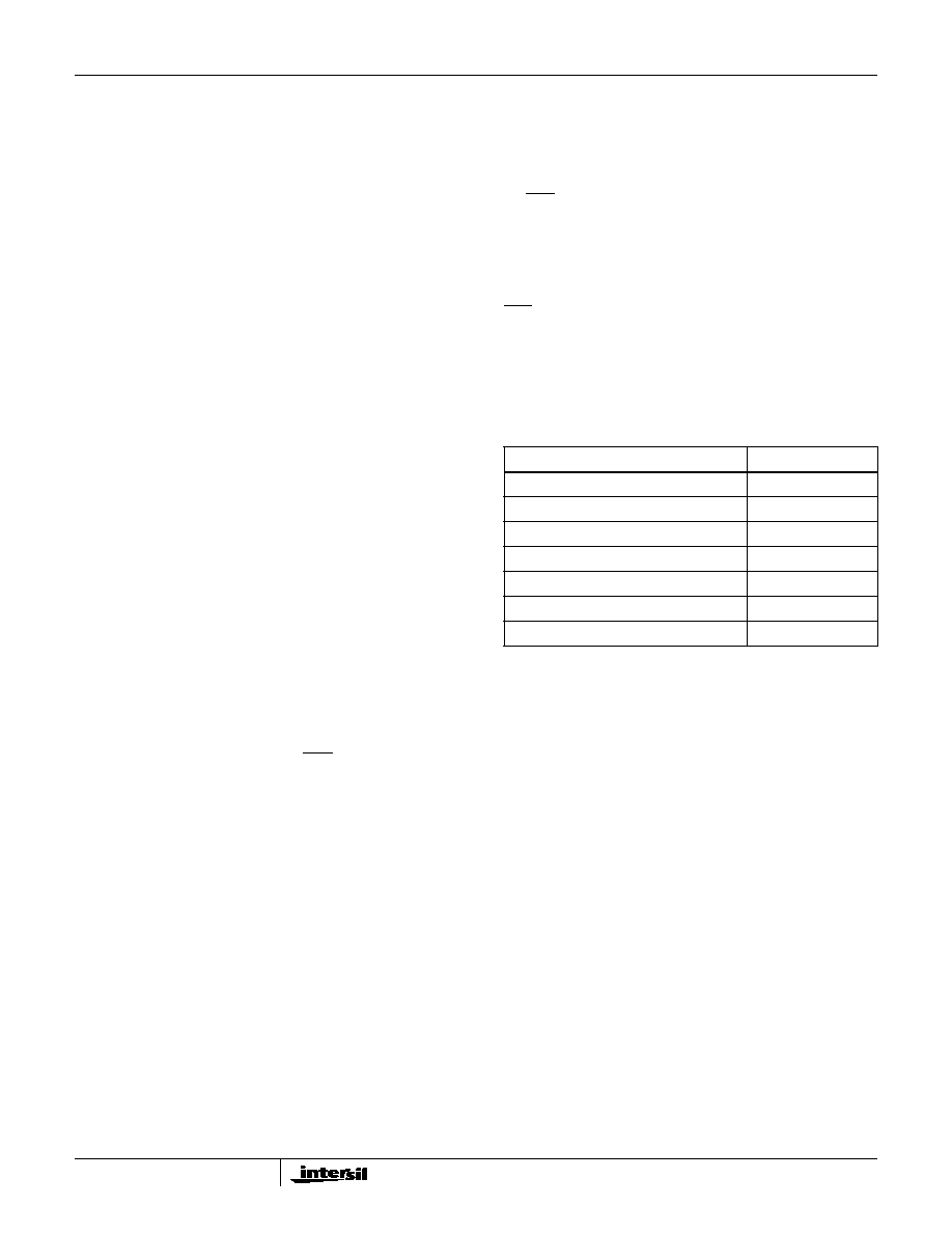
TABLE 1. REGISTER RESET VALUES
REGISTER
VALUE (HEX)
Data Output Registers
XXXX (undefined)
Channel Configuration Register #2
00XXXXXX
Channel Configuration Register #1
XXXXXXXX
Control Register
0000
Offset Calibration Registers
000000
Positive Full Scale Calibration Registers
800000
Negative Full Scale Calibration Registers
800000
HI7188
相关PDF资料 |
PDF描述 |
|---|---|
| HI7190IP | IC ADC 24BIT PROGBL SER 20-PDIP |
| HI7191IP | IC ADC 24BIT PROGBL SER 20-PDIP |
| HI9P5701K-5 | CONV A/D 6BIT 30MSPS 18-SOIC |
| HMC700LP4E | IC FRACT-N PLL 16BIT 24QFN |
| HMC703LP4E | IC FRACT-N PLL W/SWEEPR 24QFN |
相关代理商/技术参数 |
参数描述 |
|---|---|
| HI7188IP | 制造商:Rochester Electronics LLC 功能描述:- Bulk 制造商:Analog Devices 功能描述:IC 16BIT ADC 7188 DIP40 制造商:Harris Corporation 功能描述: |
| HI7190 | 制造商:INTERSIL 制造商全称:Intersil Corporation 功能描述:null24-Bit, High Precision, Sigma Delta A/D Converter |
| HI7190 WAF | 制造商:Harris Corporation 功能描述: |
| HI7190_06 | 制造商:INTERSIL 制造商全称:Intersil Corporation 功能描述:24-Bit, High Precision, Sigma Delta A/D Converter |
| HI7190EVAL | 功能描述:EVALUATION PLATFORM HI7190 RoHS:否 类别:编程器,开发系统 >> 评估板 - 模数转换器 (ADC) 系列:- 产品培训模块:Obsolescence Mitigation Program 标准包装:1 系列:- ADC 的数量:1 位数:12 采样率(每秒):94.4k 数据接口:USB 输入范围:±VREF/2 在以下条件下的电源(标准):- 工作温度:-40°C ~ 85°C 已用 IC / 零件:MAX11645 已供物品:板,软件 |
发布紧急采购,3分钟左右您将得到回复。