参数资料
| 型号: | HI7188IN |
| 厂商: | Intersil |
| 文件页数: | 4/24页 |
| 文件大小: | 0K |
| 描述: | CONV A/D 16BIT 8:1 MUX 44-MQFP |
| 标准包装: | 96 |
| 位数: | 16 |
| 采样率(每秒): | 240 |
| 数据接口: | QSPI?,串行,SPI? |
| 转换器数目: | 1 |
| 功率耗散(最大): | 50mW |
| 电压电源: | 模拟和数字,双 ± |
| 工作温度: | -40°C ~ 85°C |
| 安装类型: | 表面贴装 |
| 封装/外壳: | 44-QFP |
| 供应商设备封装: | 44-MQFP(10x10) |
| 包装: | 管件 |
| 输入数目和类型: | 8 个差分,单极;8 个差分,双极 |
12
Where CS is the internal sampling capacitance and FS is the
modulator sampling rate set by the master clock divided by
six (FS = 3.6864MHz/6 = 614.4kHz).
Bipolar/Unipolar Input Ranges
The inputs can accept either unipolar or bipolar input
voltages with each physical channel’s mode being
independent of other physical channels. Bipolar or unipolar
options are chosen by programming the bipolar/unipolar
(B/U) bits of the Channel Conguration Registers (CCR).
Programming the logical channels for either unipolar or
bipolar operation does not change any of the input signal
conditioning. The inputs are differential, and as a result are
referenced to the voltage on the VINL input. For example, if
VINHX is +3.75V and logical channel X is congured for
unipolar operation with a gain of 1 and a VREF of +2.5V, the
input voltage range on the VINLX input is +1.25V to +3.75V. If
VINLX is +1.25V and logical channel X is congured for
bipolar mode with gain of 1 and a VREF of +2.5V, the analog
input range on the VINHX input is -1.25V to +3.75V.
Multiplexer
The input multiplexer is a fully differential 8 channel device
controlled by the internal microsequencer. Any number of
inputs, up to 8, can be scanned and both the number of
physical channels scanned and the scanning order are
controlled by the users programming of the Channel
Configuration Register (CCR). The output of the multiplexer
feeds the input to the Programmable Gain Instrumentation
Amplifier (PGIA).
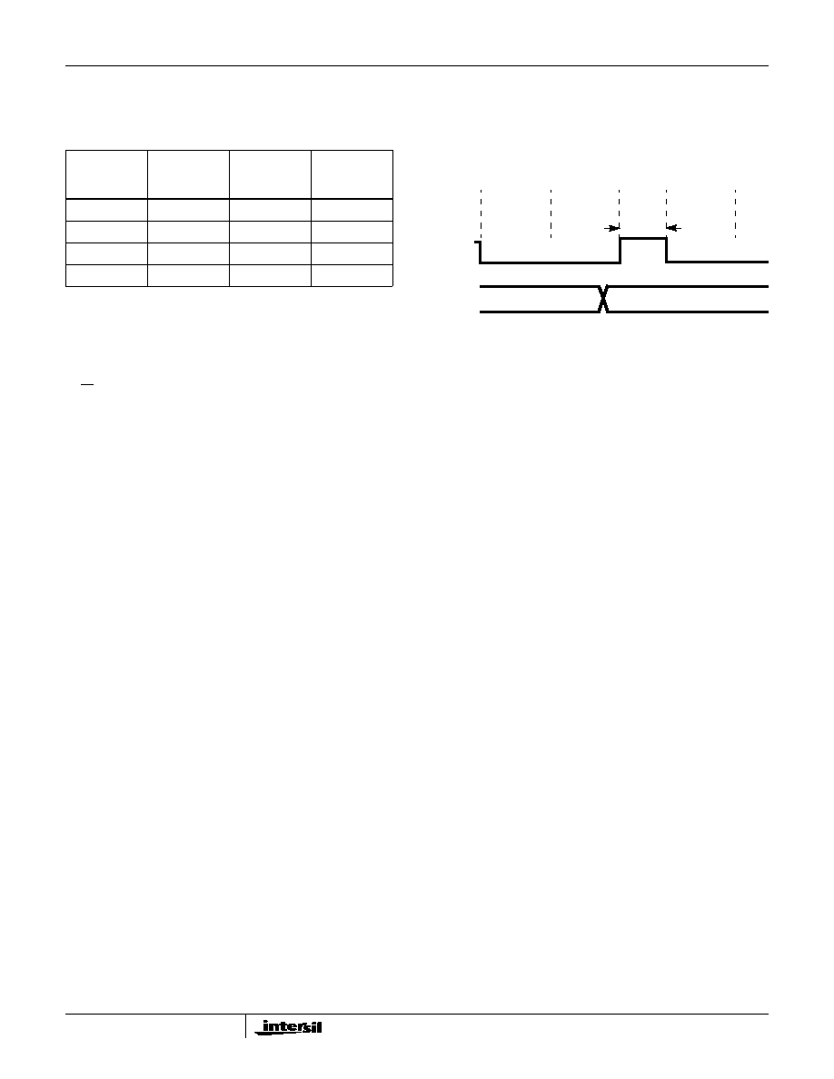
External Multiplexers
For interfacing the HI7188 to external multiplexers several
output pins are available. These pins include MXC, A2, A1
and A0. Refer to Figure 9. The MXC pulse is active high
during the modulator and integrating lter reset pulse. The
pulse width is typically 14.6
s with LNR disabled and 54.6s
with LNR enabled. This signal can be used to “break before
make” an external multiplexer. Referring to Figure 9, the data
conversion time involves the actual input channel A/D
conversion while the calibration time involves data
calibration and coding of the conversion results. The address
pins A2, A1 and A0 describe the logical address which is
currently being converted. The user can utilize these output
pins to drive external multiplexer address pins.
The main critical issue is the external multiplexer output
must switch and settle to 0.00153% (16 bits) of the nal
value during the MXC reset pulse and prior to Data
Integration or data errors will occur. The input must be stable
only during the data integration period but can be changed
during the calibration period.
Programmable Gain Instrumentation Amplier
The Programmable Gain Instrumentation Amplier (PGIA)
allows the user to interface low level sensors and bridges
directly to the HI7188. The PGIA has 4 selectable gain
options of 1, 2, 4, and 8. The gain of each physical channel
is independent of other physical channels and is
programmable by writing the G1 and G0 bits in the Channel
Conguration Registers (CCR).
Differential Reference Input
The reference inputs, VRHI and VRLO, provide a differential
reference input capability. VRHI must always be greater than
VRLO for proper operation of the device. The common mode
range for these differential inputs is from AVSS to AVDD and
the nominal differential voltage (VREF = VRHI - VRLO) is
+2.5V. Larger values of VREF can be used with minor
degradation in performance. Smaller values of VREF can
also be used but performance will be degraded since the
system noise is larger relative to the LSB size. The full scale
range of the HI7188 is dened as:
FSRBIPOLAR = 2 x VREF/GAIN
FSRUNIPOLAR = VREF/GAIN
The reference inputs provide a high impedance dynamic
load similar to the analog inputs. For proper circuit operation
these pins must be driven by low impedance circuitry.
Reference noise outside of the band of interest will be
removed by the digital lter but excessive reference noise
inside the band of interest will degrade performance.
VCM Input
The VCM input is the internal reference voltage for the
HI7188 analog circuitry and should always be tied to the
midpoint of the AVDD and AVSS supplies. This point
provides a common mode input voltage for the internal
operational ampliers and must be driven from a low noise,
low impedance source if it is not tied to analog ground.
Failure to do so will result in degraded HI7188 performance.
TABLE 2. EFFECTIVE INPUT IMPEDANCE vs GAIN
GAIN
SAMPLING
RATE
(kHz)
SAMPLING
CAPACITOR
(pF)
INPUT
IMPEDANCE
(k
)
1
614.4
4
407
2
614.4
8
203
4
614.4
16
102
8
614.4
32
51
CADDR
DATA
CONVERSION CALIBRATION
CHAN
SWITCH
MXC
A2, 1, 0
DATA
CONVERSION
VALID LOGICAL ADDRESS
tMXC
FIGURE 9. CHANNEL SWITCHING TIMING
HI7188
相关PDF资料 |
PDF描述 |
|---|---|
| HI7190IP | IC ADC 24BIT PROGBL SER 20-PDIP |
| HI7191IP | IC ADC 24BIT PROGBL SER 20-PDIP |
| HI9P5701K-5 | CONV A/D 6BIT 30MSPS 18-SOIC |
| HMC700LP4E | IC FRACT-N PLL 16BIT 24QFN |
| HMC703LP4E | IC FRACT-N PLL W/SWEEPR 24QFN |
相关代理商/技术参数 |
参数描述 |
|---|---|
| HI7188IP | 制造商:Rochester Electronics LLC 功能描述:- Bulk 制造商:Analog Devices 功能描述:IC 16BIT ADC 7188 DIP40 制造商:Harris Corporation 功能描述: |
| HI7190 | 制造商:INTERSIL 制造商全称:Intersil Corporation 功能描述:null24-Bit, High Precision, Sigma Delta A/D Converter |
| HI7190 WAF | 制造商:Harris Corporation 功能描述: |
| HI7190_06 | 制造商:INTERSIL 制造商全称:Intersil Corporation 功能描述:24-Bit, High Precision, Sigma Delta A/D Converter |
| HI7190EVAL | 功能描述:EVALUATION PLATFORM HI7190 RoHS:否 类别:编程器,开发系统 >> 评估板 - 模数转换器 (ADC) 系列:- 产品培训模块:Obsolescence Mitigation Program 标准包装:1 系列:- ADC 的数量:1 位数:12 采样率(每秒):94.4k 数据接口:USB 输入范围:±VREF/2 在以下条件下的电源(标准):- 工作温度:-40°C ~ 85°C 已用 IC / 零件:MAX11645 已供物品:板,软件 |
发布紧急采购,3分钟左右您将得到回复。