参数资料
| 型号: | HI7188IN |
| 厂商: | Intersil |
| 文件页数: | 14/24页 |
| 文件大小: | 0K |
| 描述: | CONV A/D 16BIT 8:1 MUX 44-MQFP |
| 标准包装: | 96 |
| 位数: | 16 |
| 采样率(每秒): | 240 |
| 数据接口: | QSPI?,串行,SPI? |
| 转换器数目: | 1 |
| 功率耗散(最大): | 50mW |
| 电压电源: | 模拟和数字,双 ± |
| 工作温度: | -40°C ~ 85°C |
| 安装类型: | 表面贴装 |
| 封装/外壳: | 44-QFP |
| 供应商设备封装: | 44-MQFP(10x10) |
| 包装: | 管件 |
| 输入数目和类型: | 8 个差分,单极;8 个差分,双极 |
21
bipolar/unipolar operation. The 64 bits are divided into two 32
bit register blocks referred to as CCR#2 and CCR#1. Each
register contains four bytes pertaining to four logical channels.
The register may be accessed 1, 2, 3 or 4 bytes at a time.
Please refer to Table 10 to determine physical address
assignments within the CCR and Table 9 for logical channel
assignment. The physical channel conversion order is defined
based on it’s location in the CCR blocks. For example, if the
CCR #2 <31:24> is set with the CCR <2:0> = 100, then
physical channel 5 will be converted first. The CCR is byte wide
accessible via the Serial Interface allowing the user to change
the individual logical channel configuration on the fly. Following
are the bit assignments.
CH2, CH1, CH0 - Bits 7, 6, 5 of the channel configuration byte
determine which physical inputs are used as shown in Table 10.
B/U - Bit 4 of the channel conguration byte determine
bipolar or unipolar mode. If Logic 1, bipolar mode is selected
while logic 0 selects unipolar mode.
MD1, MD0 - Bit 3 and 2 of the channel conguration byte are
the channel Mode bits. This denes the mode of operation
for that logical channel, please see Table 11. All calibration
modes automatically return to conversion mode after
calibration is complete.
G1, G0 - Bit 1 and 0 denes the PGIA gain of 1, 2, 4 or 8.
Please refer to Table 12.
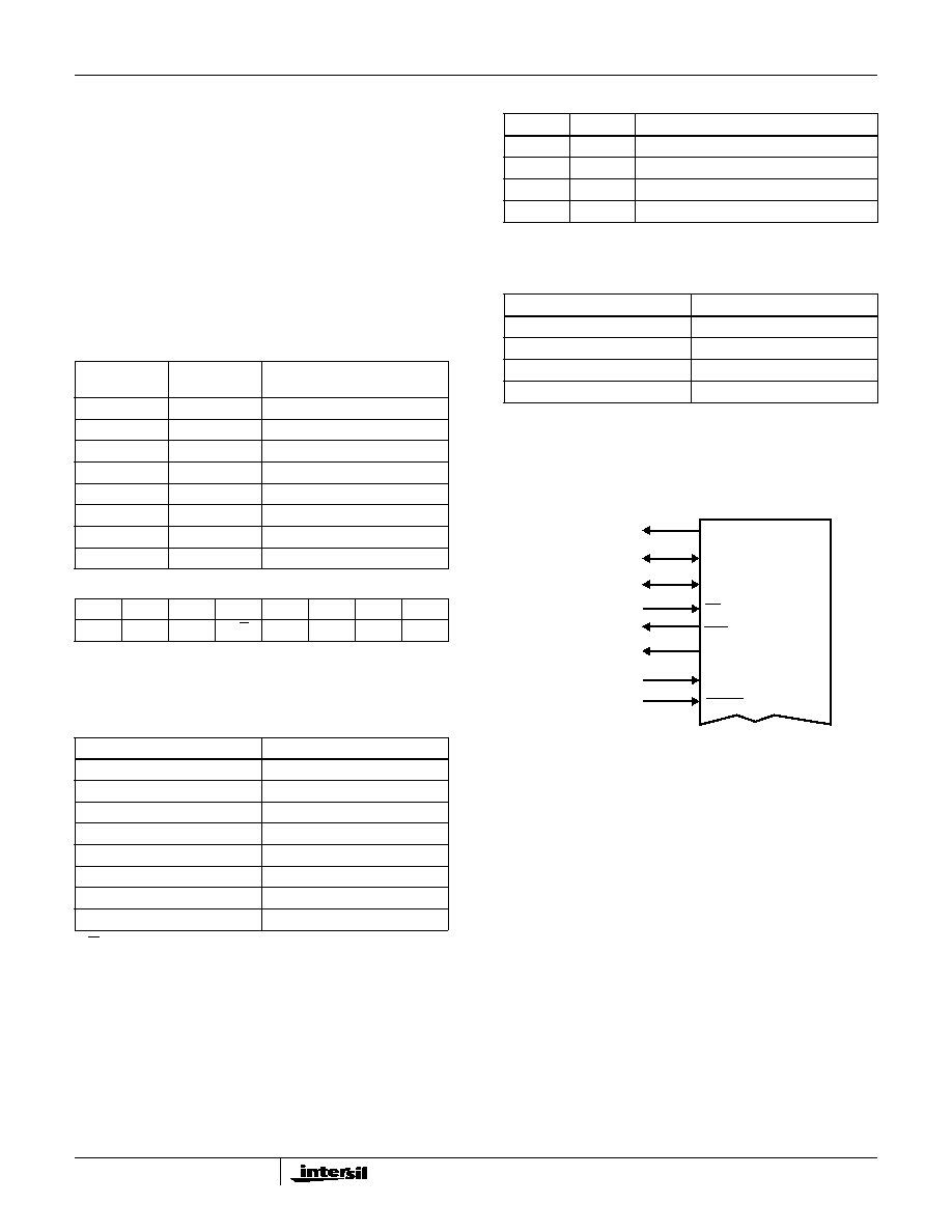
Serial Interface Pin Description
The serial I/O port is a bidirectional port which is used to
read and write the internal registers. The port contains two
data lines, a synchronous clock, and two status ags.
Figure 14 shows a diagram of the serial interface lines.
SDO - Serial Data Out. Data is read from this line using those
protocols with separate lines for transmitting and receiving
data. An example of such a standard is the Motorola Serial
Peripheral Interface (SPI) using the 68HC05 and 68HC11
family of microcontrollers, or other similar processors. In the
case of using bidirectional data transfer on SDIO, the SDO
does not output data and is set in a high impedance state.
SDIO. Serial Data In or Out. Data is always written to the
device on this line. However, this line can be used as a
bidirectional data line. This is done by properly setting up the
Control Register. Bidirectional data transfer on this line can
be used with Intel standard serial interfaces (SSR, Mode 0)
in MCS51 and MCS96 family of microcontrollers, or other
similar processors.
SCLK. Serial Clock. The serial clock pin is used to
synchronize data to and from the HI7188 and to run the port
state machines. In Synchronous External Clock Mode, SCLK
is configured as an input, is supplied by the user, and can run
up to a 5MHz rate. In Synchronous Self Clocking Mode, SCLK
is configured as an output and runs at OSC1/8 = 460.8kHz.
TABLE 9. CHANNEL CONFIGURATION REGISTER
BLOCK
BIT
LOCATION
DESCRIPTION
CCR #2
<31:24>
1st Logical Channel
CCR #2
<23:16>
2nd Logical Channel
CCR #2
<15:8>
3rd Logical Channel
CCR #2
<7:0>
4th Logical Channel
CCR #1
<31:24>
5th Logical Channel
CCR #1
<23:16>
6th Logical Channel
CCR #1
<15:8>
7th Logical Channel
CCR #1
<7:0>
8th Logical Channel
CHANNEL CONFIGURATION REGISTER (BYTE)
MSB
654321
LSB
CH2
CH1
CH0
B/U
MD1
MD0
G1
G0
TABLE 10. ACTIVE CHANNEL DECODE
CH2, CH1, CH0 CCR [2:0]
PHYSICAL INPUT PINS
000
VINH1, VINL1
001
VINH2, VINL2
010
VINH3, VINL3
011
VINH4, VINL4
100
VINH5, VINL5
101
VINH6, VINL6
110
VINH7, VINL7
111
VINH8, VINL8
TABLE 11. HI7188 OPERATIONAL MODES
MD1
MD0
OPERATIONAL MODE
0
Conversion
0
1
System Offset Calibration
1
0
System Positive Full Scale Calibration
1
System Negative Full Scale Calibration
TABLE 12. CHANNEL GAIN
G1, G0 CCR [1:0]
PGIA CHANNEL GAIN
00
1
01
2
10
4
11
8
SDO
SDIO
SCLK
CS
EOS
CHIP SELECT
BIDIRECTIONAL
DATA
DATA OUT
PORT CLOCK
CA
CALIBRATION
MODE
CLOCK MODE
ACTIVE
END OF SCAN
HI7188
RSTI/O
RESET I/O
FIGURE 14. HI7188 SERIAL INTERFACE
HI7188
相关PDF资料 |
PDF描述 |
|---|---|
| HI7190IP | IC ADC 24BIT PROGBL SER 20-PDIP |
| HI7191IP | IC ADC 24BIT PROGBL SER 20-PDIP |
| HI9P5701K-5 | CONV A/D 6BIT 30MSPS 18-SOIC |
| HMC700LP4E | IC FRACT-N PLL 16BIT 24QFN |
| HMC703LP4E | IC FRACT-N PLL W/SWEEPR 24QFN |
相关代理商/技术参数 |
参数描述 |
|---|---|
| HI7188IP | 制造商:Rochester Electronics LLC 功能描述:- Bulk 制造商:Analog Devices 功能描述:IC 16BIT ADC 7188 DIP40 制造商:Harris Corporation 功能描述: |
| HI7190 | 制造商:INTERSIL 制造商全称:Intersil Corporation 功能描述:null24-Bit, High Precision, Sigma Delta A/D Converter |
| HI7190 WAF | 制造商:Harris Corporation 功能描述: |
| HI7190_06 | 制造商:INTERSIL 制造商全称:Intersil Corporation 功能描述:24-Bit, High Precision, Sigma Delta A/D Converter |
| HI7190EVAL | 功能描述:EVALUATION PLATFORM HI7190 RoHS:否 类别:编程器,开发系统 >> 评估板 - 模数转换器 (ADC) 系列:- 产品培训模块:Obsolescence Mitigation Program 标准包装:1 系列:- ADC 的数量:1 位数:12 采样率(每秒):94.4k 数据接口:USB 输入范围:±VREF/2 在以下条件下的电源(标准):- 工作温度:-40°C ~ 85°C 已用 IC / 零件:MAX11645 已供物品:板,软件 |
发布紧急采购,3分钟左右您将得到回复。