- 您现在的位置:买卖IC网 > PDF目录16296 > LTC4110EUHF#PBF (Linear Technology)IC BATTERY BACKUP MANAGER 38-QFN PDF资料下载
参数资料
| 型号: | LTC4110EUHF#PBF |
| 厂商: | Linear Technology |
| 文件页数: | 47/52页 |
| 文件大小: | 0K |
| 描述: | IC BATTERY BACKUP MANAGER 38-QFN |
| 标准包装: | 52 |
| 功能: | 备份管理 |
| 电池化学: | 铅酸,锂离子,锂聚合物,镍镉,镍氢,超级电容器 |
| 电源电压: | 4.5 V ~ 19 V |
| 工作温度: | -40°C ~ 85°C |
| 安装类型: | 表面贴装 |
| 封装/外壳: | 38-WFQFN 裸露焊盘 |
| 供应商设备封装: | 38-QFN(5x7) |
| 包装: | 管件 |
| 产品目录页面: | 1341 (CN2011-ZH PDF) |
第1页第2页第3页第4页第5页第6页第7页第8页第9页第10页第11页第12页第13页第14页第15页第16页第17页第18页第19页第20页第21页第22页第23页第24页第25页第26页第27页第28页第29页第30页第31页第32页第33页第34页第35页第36页第37页第38页第39页第40页第41页第42页第43页第44页第45页第46页当前第47页第48页第49页第50页第51页第52页
�� �
�
�LTC4110�
�APPLICATIONS� INFORMATION�
�PCB� LAYOUT� CONSIDERATIONS�
�For� maximum� ef?ciency,� the� switch� node� rise� and� fall�
�times� should� be� minimized.� To� prevent� magnetic� and�
�electrical� ?eld� (EMI)� radiation� and� high� frequency� resonant�
�problems,� proper� layout� of� the� components� connected� to�
�the� IC� is� essential.�
�Flyback� Layout�
�Lowest� EMI� and� maximum� ef?ciency� are� obtained� when� the�
�high� frequency� switching� current� loop� area� is� minimized.�
�It� is� best� to� make� direct� connections,� avoiding� the� use� of�
�other� circuit� board� copper� planes,� i.e.� no� vias,� in� making�
�the� following� connections� for� this� prevents� current� based�
�noise� injection� into� the� copper� planes� below.�
�1.� Input/output� capacitors� positive� terminals� need� to�
�be� placed� as� close� as� possible� between� the� ?yback�
�transformer� “top”� or� positive� supply� rail� connections�
�and� R� SNS(FET)� ground� connection.�
�2.� Place� ?yback� MOSFETs� drain� connections� right� next�
�to� the� ?yback� transformers� “bottom”� connections.�
�3.� Place� the� R� SNS(FET)� current� sense� resistor� right� next�
�to� the� N-MOSFET� source� connections� completing�
�the� connection� back� to� the� input/output� capacitors’�
�negative� terminals.�
�4.� Place� the� snubber� connections� as� close� as� possible�
�to� the� circuit� after� the� above� layout� connections� are�
�completed� as� required.� Again,� avoid� using� vias.�
�5.� The� layer� below� the� ?yback� layout� should� be� ground.�
�Other� Recommendations�
�6.� Optionally� use� vias� to� connect� power� supply� sources�
�positive� and� negative� (ground)� connections� from�
�other� copper� layers� to� the� ?yback� layout.� Place�
�multiple� vias� in� a� tight� cluster� such� that� they� act� as�
�one� large� via.� Recommended� 1� via� for� each� 0.5A� of�
�current�
�7.� The� current� sense� feedback� traces� must� be� routed�
�together� as� a� single� pair� on� the� same� layer� at� any�
�given� time� with� smallest� trace� spacing� possible.�
�Locate� any� ?lter� component� on� these� traces� next� to�
�the� IC� and� not� at� the� sense� resistor� location.�
�8.� The� control� IC� must� be� close� to� the� switching� FET’s�
�gate� terminals.� Keep� the� gate� drive� signals� short� for�
�a� clean� FET� drive.� This� includes� IC� supply� pins� that�
�connect� to� the� switching� FET� source� pins.� The� IC� can�
�be� placed� on� the� opposite� side� of� the� PCB� relative� to�
�?yback� layout� above.�
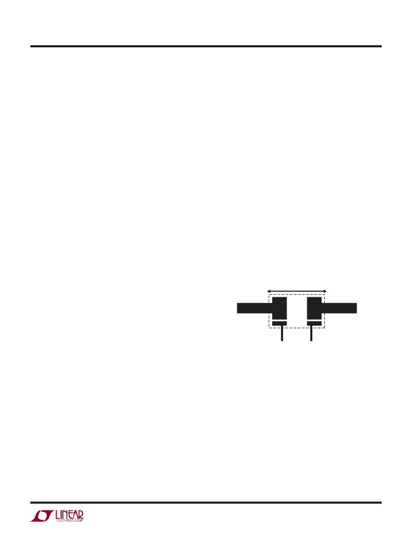
�9.� Figure� 21� shows� an� inexpensive� way� to� achieve�
�Kelvin� like� sensing� using� standard� current� sense�
�resistors.�
�DIRECTION� OF� CHARGING� CURRENT�
�R� SNS(BAT)�
�4110� F21�
�TO� CSP� AND� CSN�
�Figure� 21.� Kelvin� Sensing� of� Battery� Current�
�4110fb�
�47�
�相关PDF资料 |
PDF描述 |
|---|---|
| 3-6754412-6 | CA,XG,MTRJ-SC |
| ECO-S2DB102EA | CAP ALUM 1000UF 200V 20% SNAP |
| 3-6754411-6 | CA,XG,MTRJ-SC |
| RCM10DRYI-S13 | CONN EDGECARD 20POS .156 EXTEND |
| ECO-S2WB181DA | CAP ALUM 180UF 450V 20% SNAP |
相关代理商/技术参数 |
参数描述 |
|---|---|
| LTC4110EUHF-TR | 制造商:LINER 制造商全称:Linear Technology 功能描述:Battery Backup System Manager |
| LTC4110EUHF-TRPBF | 制造商:LINER 制造商全称:Linear Technology 功能描述:Battery Backup System Manager |
| LTC4120IUD#PBF | 制造商:Linear Technology 功能描述:BATTERY CHARGER, 400MA, QFN-16, Battery Type:Li-Ion, Li-Polymer, Input Voltage:4 |
| LTC4150 | 制造商:LINER 制造商全称:Linear Technology 功能描述:High Voltage, High-Side Current Sense |
| LTC4150_1 | 制造商:LINER 制造商全称:Linear Technology 功能描述:Coulomb Counter/ Battery Gas Gauge |
发布紧急采购,3分钟左右您将得到回复。