- 您现在的位置:买卖IC网 > PDF目录224123 > M25P40-VMN6TG/X (NUMONYX) 512K X 8 SPI BUS SERIAL EEPROM, PDSO8 PDF资料下载
参数资料
| 型号: | M25P40-VMN6TG/X |
| 厂商: | NUMONYX |
| 元件分类: | PROM |
| 英文描述: | 512K X 8 SPI BUS SERIAL EEPROM, PDSO8 |
| 封装: | 0.150 INCH, ROHS COMPLIANT, PLASTIC, SOP-8 |
| 文件页数: | 6/57页 |
| 文件大小: | 1160K |
| 代理商: | M25P40-VMN6TG/X |
第1页第2页第3页第4页第5页当前第6页第7页第8页第9页第10页第11页第12页第13页第14页第15页第16页第17页第18页第19页第20页第21页第22页第23页第24页第25页第26页第27页第28页第29页第30页第31页第32页第33页第34页第35页第36页第37页第38页第39页第40页第41页第42页第43页第44页第45页第46页第47页第48页第49页第50页第51页第52页第53页第54页第55页第56页第57页
Operating features
M25P40
14/57
4.7
Hold condition
The Hold (HOLD) signal is used to pause any serial communications with the device without
resetting the clocking sequence. However, taking this signal Low does not terminate any
Write Status Register, Program or Erase cycle that is currently in progress.
To enter the Hold condition, the device must be selected, with Chip Select (S) Low.
The Hold condition starts on the falling edge of the Hold (HOLD) signal, provided that this
coincides with Serial Clock (C) being Low (as shown in Figure 5).
The Hold condition ends on the rising edge of the Hold (HOLD) signal, provided that this
coincides with Serial Clock (C) being Low.
If the falling edge does not coincide with Serial Clock (C) being Low, the Hold condition
starts after Serial Clock (C) next goes Low. Similarly, if the rising edge does not coincide
with Serial Clock (C) being Low, the Hold condition ends after Serial Clock (C) next goes
Low. (This is shown in Figure 5).
During the Hold condition, the Serial Data output (Q) is high impedance, and Serial Data
input (D) and Serial Clock (C) are Don’t Care.
Normally, the device is kept selected, with Chip Select (S) driven Low, for the whole duration
of the Hold condition. This is to ensure that the state of the internal logic remains unchanged
from the moment of entering the Hold condition.
If Chip Select (S) goes High while the device is in the Hold condition, this has the effect of
resetting the internal logic of the device. To restart communication with the device, it is
necessary to drive Hold (HOLD) High, and then to drive Chip Select (S) Low. This prevents
the device from going back to the Hold condition.
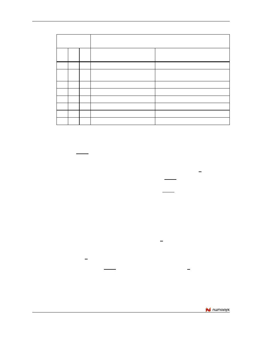
Table 2.
Protected area sizes
Status Register
content
Memory content
BP2
bit
BP1
bit
BP0
bit
Protected area
Unprotected area
0
none
All sectors(1) (eight sectors: 0 to 7)
1. The device is ready to accept a Bulk Erase instruction if, and only if, all Block Protect (BP2, BP1, BP0) are
0.
0
1
Upper eighth (Sector 7)
Lower seven-eighths (seven sectors: 0 to
6)
0
1
0
Upper quarter (two sectors: 6 and 7) Lower three-quarters (six sectors: 0 to 5)
0
1
Upper half (four sectors: 4 to 7)
Lower half (four sectors: 0 to 3)
1
0
All sectors (eight sectors: 0 to 7)
none
1
0
1
All sectors (eight sectors: 0 to 7)
none
1
0
All sectors (eight sectors: 0 to 7)
none
1
All sectors (eight sectors: 0 to 7)
none
相关PDF资料 |
PDF描述 |
|---|---|
| M25P40VMF6 | 4 Mbit Uniform Sector, Serial Flash Memory |
| M25P40VMF6G | 4 Mbit Uniform Sector, Serial Flash Memory |
| M25P40VMF6P | 4 Mbit Uniform Sector, Serial Flash Memory |
| M25P40VMF6T | 4 Mbit Uniform Sector, Serial Flash Memory |
| M25P40VMF6TG | 4 Mbit Uniform Sector, Serial Flash Memory |
相关代理商/技术参数 |
参数描述 |
|---|---|
| M25P40VMN6TP | 制造商:STMICROELECTRONICS 制造商全称:STMicroelectronics 功能描述:512 Kbit to 32 Mbit, Low Voltage, Serial Flash Memory With 40 MHz or 50 MHz SPI Bus Interface |
| M25P40-VMN6TP | 功能描述:闪存 SERIAL SECTOR ERASE FLASH 4MEG RoHS:否 制造商:ON Semiconductor 数据总线宽度:1 bit 存储类型:Flash 存储容量:2 MB 结构:256 K x 8 定时类型: 接口类型:SPI 访问时间: 电源电压-最大:3.6 V 电源电压-最小:2.3 V 最大工作电流:15 mA 工作温度:- 40 C to + 85 C 安装风格:SMD/SMT 封装 / 箱体: 封装:Reel |
| M25P40-VMN6TP/X | 制造商:NUMONYX 制造商全称:Numonyx B.V 功能描述:4 Mbit, low voltage, serial Flash memory with 50 MHz SPI bus interface |
| M25P40-VMN6TP_NUD | 制造商:Micron Technology Inc 功能描述: |
| M25P40-VMN6TPB | 功能描述:IC FLASH 4MBIT 75MHZ 8SOIC RoHS:是 类别:集成电路 (IC) >> 存储器 系列:Forté™ 标准包装:2,000 系列:- 格式 - 存储器:RAM 存储器类型:SRAM - 异步 存储容量:256K (32K x 8) 速度:15ns 接口:并联 电源电压:3 V ~ 3.6 V 工作温度:-40°C ~ 85°C 封装/外壳:28-TSSOP(0.465",11.8mm 宽) 供应商设备封装:28-TSOP 包装:带卷 (TR) 其它名称:71V256SA15PZGI8 |
发布紧急采购,3分钟左右您将得到回复。