- 您现在的位置:买卖IC网 > PDF目录359020 > M295V200T-55M1R (意法半导体) CONNECTOR ACCESSORY PDF资料下载
参数资料
| 型号: | M295V200T-55M1R |
| 厂商: | 意法半导体 |
| 英文描述: | CONNECTOR ACCESSORY |
| 中文描述: | 连接器附件 |
| 文件页数: | 3/33页 |
| 文件大小: | 224K |
| 代理商: | M295V200T-55M1R |
第1页第2页当前第3页第4页第5页第6页第7页第8页第9页第10页第11页第12页第13页第14页第15页第16页第17页第18页第19页第20页第21页第22页第23页第24页第25页第26页第27页第28页第29页第30页第31页第32页第33页
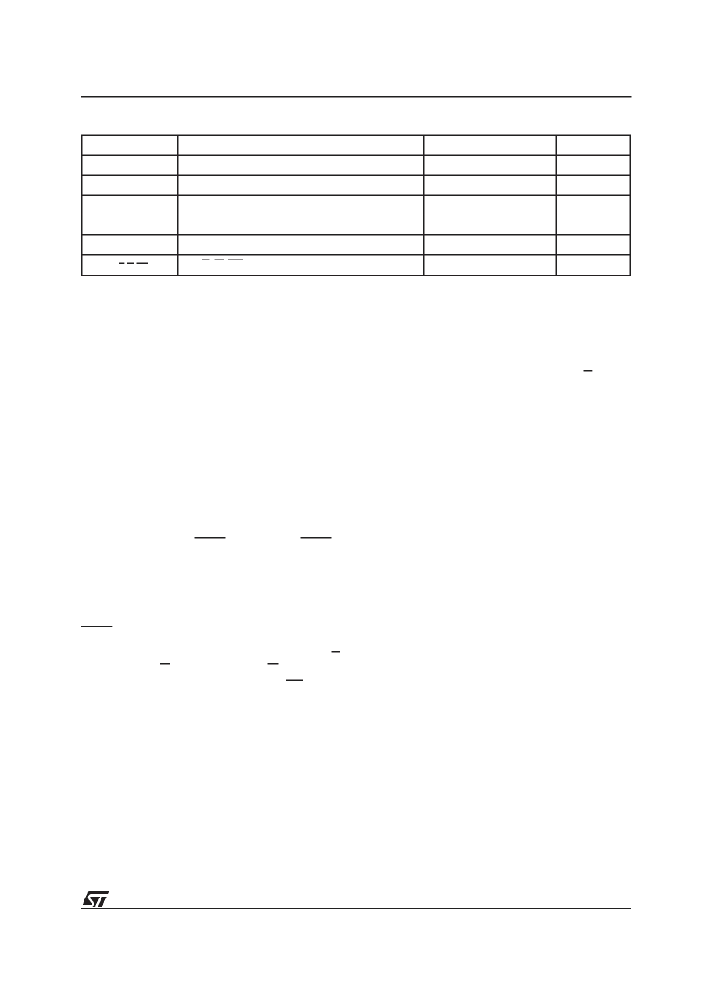
Symbol
Parameter
Value
Unit
T
A
Ambient Operating Temperature
(3)
–40 to 125
°
C
T
BIAS
Temperature Under Bias
–50 to 125
°
C
T
STG
V
IO(2)
Storage Temperature
–65 to 150
°
C
Input or Output Voltages
–0.6to 7
V
V
CC
Supply Voltage
–0.6to 7
V
V
(A9, E, G, RP)
(2)
A9, E, G, RP Voltage
–0.6to 13.5
V
Notes:
1. Except for therating ”Operating Temperature Range”, stresses above those listed in theTable ”AbsoluteMaximum Ratings”
may cause permanentdamage to thedevice. These are stress ratings only and operation of the device at these or any other
conditions above those indicated in the Operatingsections of this specification is not implied.Exposure to Absolute Maximum
Rating conditions for extendedperiods may affectdevice reliability.Refer also tothe STMicroelectronics SURE Program and other
relevant quality documents.
2. Minimum Voltagemay undershoot to –2V during transitionand for less than 20ns.
3. Depends on range.
Table2. Absolute MaximumRatings
(1)
Instructions for Read/Reset,Auto Select for read-
ing the Electronic Signature or Block Protection
status,Programming,Blockand ChipErase,Erase
Suspend and Resume are written to the device in
cyclesof commandstoa CommandInterfaceusing
standardmicroprocessorwrite timings.
The device is offeredin TSOP48(12 x 20mm)and
SO44packages.Both normaland reversepinouts
are availablefor the TSOP48package.
Organisation
TheM29F200is organisedas 256Kx8or128Kx16
bitsselectableby the BYTEsignal.When BYTEis
Low theByte-wide x8 organisationis selectedand
the address lines are DQ15A–1 and A0-A16. The
Data Input/Output signal DQ15A–1 acts as ad-
dress line A–1 which selects the lower or upper
Byte of the memoryword for output on DQ0-DQ7,
DQ8-DQ14 remain at High impedance. When
BYTEis Highthe memoryuses the addressinputs
A0-A16 and the Data Input/Outputs DQ0-DQ15.
Memory control is provided by Chip Enable E,
Output Enable G and Write EnableW inputs.
AReset/BlockTemporaryUnprotection RPtri-level
input provides a hardware reset when pulled Low,
andwhenheldHigh(atV
ID
)temporarily unprotects
blocks previously protected allowing them to be
programedanderased.EraseandProgramopera-
tions are controlled by an internal Program/Erase
Controller(P/E.C.). StatusRegisterdata output on
DQ7providesa Data Pollingsignal, and DQ6and
DQ2provideToggle signalsto indicatethe stateof
the P/E.C operations. A Ready/Busy RB output
indicatesthe completionof theinternalalgorithms.
MemoryBlocks
The devicesfeature asymmetrically blockedarchi-
tectureprovidingsystemmemory integration.Both
M29F200Tand M29F200Bdevices have an array
of 7 blocks, one Boot Block of 16 KBytes or 8
KWords, two Parameter Blocks of 8 KBytes or 4
KWords, one Main Block of 32 KBytes or 16
KWordsand threeMain Blocksof 64 KBytesor 32
KWords.The M29F200Thas the BootBlockat the
top of the memory address space and the
M29F200B locates the Boot Block starting at the
bottom. The memory maps are showed in Figure
3. Each block can be erased separately,any com-
bination of blocks can be specified for multi-block
eraseor the entire chipmay beerased.The Erase
operations are managed automatically by the
P/E.C. The block erase operation can be sus-
pended in order to read from or program to any
block not beingersased, and then resumed.
Block protectionprovides additional data security.
Each block can be separatelyprotected or unpro-
tectedagainst Program or Erase on programming
equipment.All previously protected blocks can be
temporarily unprotectedin the application.
Bus Operations
The following operations can be performed using
theappropriatebus cycles:Read(Array,Electronic
Signature, Block Protection Status), Write com-
mand, OutputDisable,Standby,Reset, Block Pro-
tection, Unprotection, Protection Verify,
Unprotection Verify and Block Temporary Unpro-
tection.See Tables4 and 5.
DESCRIPTION
(Cont’d)
3/33
M29F200T, M29F200B
相关PDF资料 |
PDF描述 |
|---|---|
| M295V400T-55N6R | 4 Mbit 512Kb x8 or 256Kb x16, Boot Block Single Supply Flash Memory |
| M295V800AB90M1T | Circular Connector; No. of Contacts:37; Series:JT02R; Body Material:Aluminum; Connecting Termination:Crimp; Connector Shell Size:14; Circular Contact Gender:Socket; Circular Shell Style:Box Mount Receptacle; Insert Arrangement:14-35 |
| M29DW128F60NF1 | 128 Mbit (16Mb x8 or 8Mb x16, Multiple Bank, Page, Boot Block) 3V Supply, Flash Memory |
| M29DW128F60NF1E | 128 Mbit (16Mb x8 or 8Mb x16, Multiple Bank, Page, Boot Block) 3V Supply, Flash Memory |
| M29DW128F60NF1F | 128 Mbit (16Mb x8 or 8Mb x16, Multiple Bank, Page, Boot Block) 3V Supply, Flash Memory |
相关代理商/技术参数 |
参数描述 |
|---|---|
| M295V200T-55M1TR | 制造商:STMICROELECTRONICS 制造商全称:STMicroelectronics 功能描述:2 Mbit 256Kb x8 or 128Kb x16, Boot Block Single Supply Flash Memory |
| M295V200T-55M3R | 制造商:STMICROELECTRONICS 制造商全称:STMicroelectronics 功能描述:2 Mbit 256Kb x8 or 128Kb x16, Boot Block Single Supply Flash Memory |
| M295V200T-55M3TR | 制造商:STMICROELECTRONICS 制造商全称:STMicroelectronics 功能描述:2 Mbit 256Kb x8 or 128Kb x16, Boot Block Single Supply Flash Memory |
| M295V200T-55M6R | 制造商:STMICROELECTRONICS 制造商全称:STMicroelectronics 功能描述:2 Mbit 256Kb x8 or 128Kb x16, Boot Block Single Supply Flash Memory |
| M295V200T-55M6TR | 制造商:STMICROELECTRONICS 制造商全称:STMicroelectronics 功能描述:2 Mbit 256Kb x8 or 128Kb x16, Boot Block Single Supply Flash Memory |
发布紧急采购,3分钟左右您将得到回复。