- 您现在的位置:买卖IC网 > PDF目录359020 > M295V400T-55N6R (意法半导体) 4 Mbit 512Kb x8 or 256Kb x16, Boot Block Single Supply Flash Memory PDF资料下载
参数资料
| 型号: | M295V400T-55N6R |
| 厂商: | 意法半导体 |
| 英文描述: | 4 Mbit 512Kb x8 or 256Kb x16, Boot Block Single Supply Flash Memory |
| 中文描述: | 4兆位512KB的x8或256Kb的x16插槽,启动座单电源闪存 |
| 文件页数: | 12/34页 |
| 文件大小: | 231K |
| 代理商: | M295V400T-55N6R |
第1页第2页第3页第4页第5页第6页第7页第8页第9页第10页第11页当前第12页第13页第14页第15页第16页第17页第18页第19页第20页第21页第22页第23页第24页第25页第26页第27页第28页第29页第30页第31页第32页第33页第34页
Toggle Bit (DQ2).
This toggle bit, together with
DQ6, can be used to determine the device status
duringthe Eraseoperations. It can alsobe usedto
identify the block being erased. During Erase or
Erase Suspend a read from a block being erased
will cause DQ2 to toggle. A read from a block not
being erased will set DQ2 to ’1’during erase and
to DQ2during Erase Suspend. During Chip Erase
a read operation will cause DQ2 to toggle as all
blocks are being erased. DQ2 will be set to ’1’
duringprogram operation and whenerase iscom-
plete. After erase completion and if the error bit
DQ5 is set to ’1’,DQ2 willtoggle if thefaulty block
is addressed.
ErrorBit (DQ5).
Thisbit is set to ’1’ by the P/E.C.
when there is a failure of programming, block
erase, or chip erase that results in invalid data in
thememoryblock.Incaseofanerrorinblockerase
or program, the blockin whichthe error occured or
to which the programmed data belongs, must be
discarded. The DQ5 failure condition will also ap-
pearif a usertriesto programa ’1’to a locationthat
is previously programmed to ’0’. Other Blocksmay
stillbeused.Theerror bitresetsafteraRead/Reset
(RD) instruction. In caseof success of Programor
Erase, the error bit will be set to ’0’.
Erase Timer Bit (DQ3).
Thisbit is set to ’0’ by the
P/E.C. when the last block Erase command has
been entered to the Command Interface and it is
awaiting the Erase start. When the erase timeout
periodisfinished, after 80
μ
sto120
μ
s, DQ3returns
to ’1’.
CodedCycles
The twoCoded cycles unlock the Command Inter-
face. They are followed by an input command or a
confirmation command. The Coded cycles consist
of writing the data AAh at address AAAAh in the
Byte-wide configuration and at address 5555h in
the Word-wide configuration during the first cycle.
During the secondcycle the Coded cyclesconsist
of writing the data 55h at address 5555h in the
Byte-wide configuration and at address 2AAAh in
the Word-wideconfiguration. In theByte-widecon-
figurationtheaddress linesA–1 to A14 are valid, in
Word-wideA0 toA14are valid,other addresslines
are ’don’t care’. The Coded cycles happen on first
and secondcycles of the command write oron the
fourth and fifth cycles.
Instructions
See Table8.
Read/Reset (RD) Instruction.
The Read/Reset
instruction consists of one write cycle giving the
commandF0h.Itcanbeoptionally precededbythe
two Codedcycles.Subsequent readoperationswill
read the memory array addressed and output the
data read. Await state of 10
μ
s is necessary after
Read/Reset prior to any valid read if the memory
was in an Erase mode when the RD instruction is
given.
Auto Select (AS) Instruction.
This instruction
uses the two Coded cycles followed by one write
cycle giving the command 90h to address AAAAh
in the Byte-wide configuration or address 5555h in
the Word-wide configuration for command set-up.
A subsequent read will output the manufacturer
code and the device code or the block protection
status depending on the levels of A0 and A1. The
manufacturer code, 20h, is output when the ad-
dresseslinesA0 and A1are Low,the devicecode,
D5h for Top Boot, D6h for Bottom Boot is output
when A0 is High with A1 Low.
The AS instruction also allowsaccess to the block
protectionstatus.AftergivingtheASinstruction,A0
is set to V
IL
with A1 at V
IH
, while A12-A17 define
the address of the block to be verified. A read in
these conditions will output a 01h if the block is
protectedand a 00h if the block is not protected.
Program (PG) Instruction.
This instruction uses
four write cycles. Both for Byte-wide configuration
and for Word-wide configuration. The Program
command A0h is written to address AAAAh in the
Byte-wide configuration or to address5555h in the
Word-wideconfiguration on thethirdcycleaftertwo
Codedcycles. Afourth write operation latches the
Addresson the fallingedgeof W or Eand theData
to be written on the rising edge and starts the
P/E.C.Read operations outputthe Status Register
bits after the programming has started. Memory
programming is madeonlyby writing’0’in placeof
’1’.StatusbitsDQ6and DQ7determineif program-
mingison-goingand DQ5allowsverification ofany
possible error. Programming at an address not in
blocks being erased is also possible during erase
suspend. In this case, DQ2 will toggle at the ad-
dress being programmed.
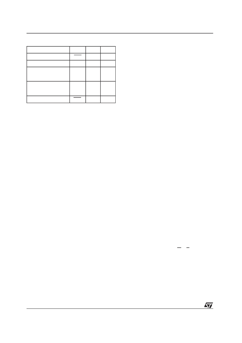
Mode
DQ7
DQ6
DQ2
Program
DQ7
Toggle
1
Erase
0
Toggle
Note 1
Erase Suspend Read
(in Erase Suspend
block)
1
1
Toggle
Erase Suspend Read
(outside Erase Suspend
block)
DQ7
DQ6
DQ2
Erase Suspend Program
DQ7
Toggle
N/A
Note:
1. Toggle if the address is within a block beingerased.
’1’ if the address is within a block not being erased.
Table 10. Pollingand Toggle Bits
12/34
M29F400T, M29F400B
相关PDF资料 |
PDF描述 |
|---|---|
| M295V800AB90M1T | Circular Connector; No. of Contacts:37; Series:JT02R; Body Material:Aluminum; Connecting Termination:Crimp; Connector Shell Size:14; Circular Contact Gender:Socket; Circular Shell Style:Box Mount Receptacle; Insert Arrangement:14-35 |
| M29DW128F60NF1 | 128 Mbit (16Mb x8 or 8Mb x16, Multiple Bank, Page, Boot Block) 3V Supply, Flash Memory |
| M29DW128F60NF1E | 128 Mbit (16Mb x8 or 8Mb x16, Multiple Bank, Page, Boot Block) 3V Supply, Flash Memory |
| M29DW128F60NF1F | 128 Mbit (16Mb x8 or 8Mb x16, Multiple Bank, Page, Boot Block) 3V Supply, Flash Memory |
| M29DW128F60NF1T | 128 Mbit (16Mb x8 or 8Mb x16, Multiple Bank, Page, Boot Block) 3V Supply, Flash Memory |
相关代理商/技术参数 |
参数描述 |
|---|---|
| M295V400T-55N6TR | 制造商:STMICROELECTRONICS 制造商全称:STMicroelectronics 功能描述:4 Mbit 512Kb x8 or 256Kb x16, Boot Block Single Supply Flash Memory |
| M295V400T-70M1R | 制造商:STMICROELECTRONICS 制造商全称:STMicroelectronics 功能描述:4 Mbit 512Kb x8 or 256Kb x16, Boot Block Single Supply Flash Memory |
| M295V400T-70M1TR | 制造商:STMICROELECTRONICS 制造商全称:STMicroelectronics 功能描述:4 Mbit 512Kb x8 or 256Kb x16, Boot Block Single Supply Flash Memory |
| M295V400T-70M3R | 制造商:STMICROELECTRONICS 制造商全称:STMicroelectronics 功能描述:4 Mbit 512Kb x8 or 256Kb x16, Boot Block Single Supply Flash Memory |
| M295V400T-70M3TR | 制造商:STMICROELECTRONICS 制造商全称:STMicroelectronics 功能描述:4 Mbit 512Kb x8 or 256Kb x16, Boot Block Single Supply Flash Memory |
发布紧急采购,3分钟左右您将得到回复。