- 您现在的位置:买卖IC网 > PDF目录370994 > M6MGB166S2BWG (Mitsubishi Electric Corporation) CMOS 3.3V-ONLY FLASH MEMORY & CMOS SRAM Stacked-CSP PDF资料下载
参数资料
| 型号: | M6MGB166S2BWG |
| 厂商: | Mitsubishi Electric Corporation |
| 英文描述: | CMOS 3.3V-ONLY FLASH MEMORY & CMOS SRAM Stacked-CSP |
| 中文描述: | 3.3的CMOS只快闪记忆体 |
| 文件页数: | 26/30页 |
| 文件大小: | 253K |
| 代理商: | M6MGB166S2BWG |
第1页第2页第3页第4页第5页第6页第7页第8页第9页第10页第11页第12页第13页第14页第15页第16页第17页第18页第19页第20页第21页第22页第23页第24页第25页当前第26页第27页第28页第29页第30页
Nov 1999 , Rev.2.3
MITSUBISHI LSIs
16,777,216-BIT (1,048,576 -WORD BY 16-BIT ) CMOS
3.3V-ONLY FLASH MEMORY &
2,097,152-BIT (131,072-WORD BY 16-BIT) CMOS SRAM
Stacked-CSP (Chip Scale Package)
M6MGB/T166S2BWG
26
AC ELECTRICAL CHARACTERISTICS
(1) TEST CONDITIONS
(S-Vcc=2.7 ~ 3.6V, unless otherwise noted)
Input rise time and fall time
Reference level
Output loads
2.7V~3.6V
V
IH
=2.2V, V
IL
=0.4V
5ns
V
OH
=V
OL
=1.5V
Transition is measured +
steady state voltage.(for t
en
,t
dis
)
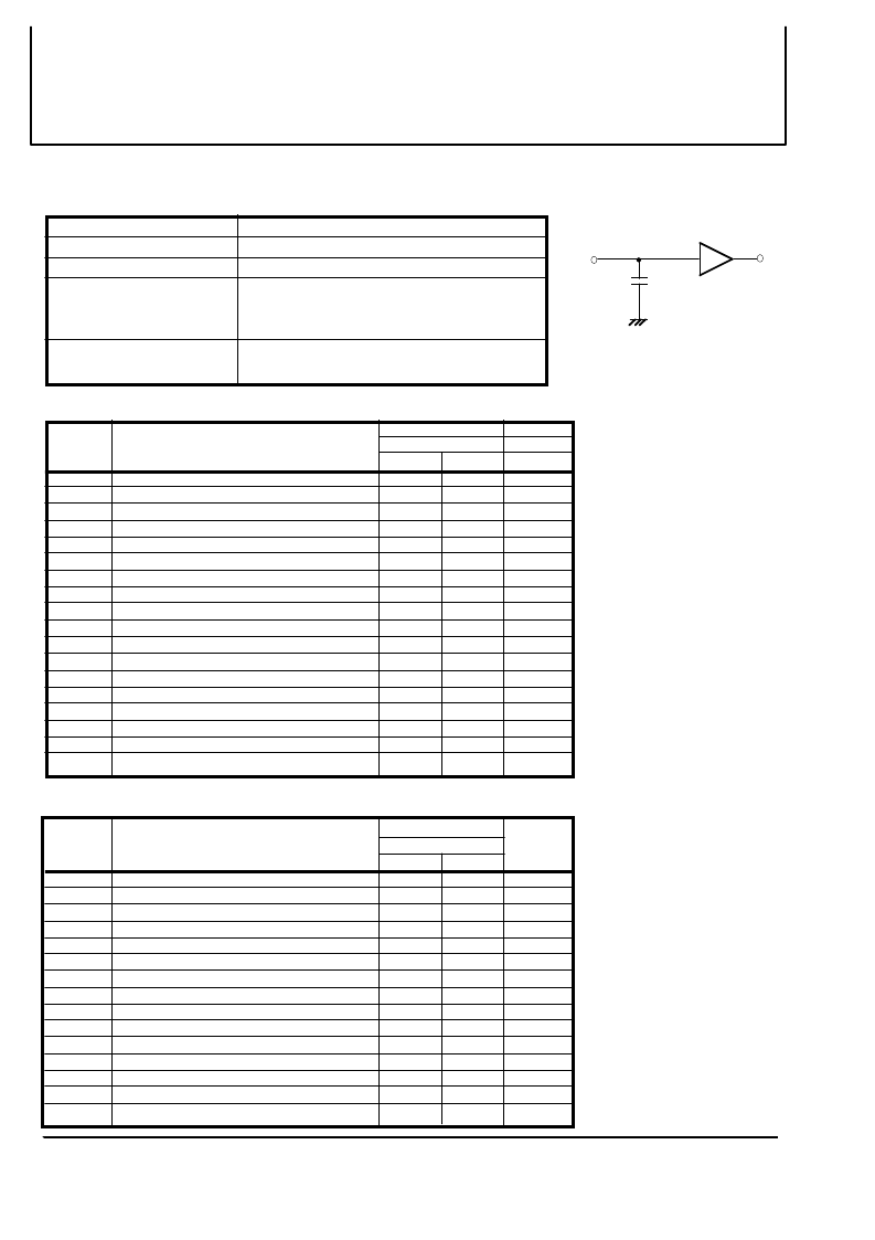
Fig.1,CL=30pF
CL=5pF (for ten,tdis)
Supply voltage
Input pulse
1TTL
CL
DQ
Fig.1 Output load
Including scope and
jig capacitance
(3) WRITE CYCLE
t
su
(A-WH)
t
su
(LB)
t
su
(UB)
t
CW
t
w
(W)
t
su
(A)
t
su
(CE1)
t
su
(CE2)
t
su
(D)
t
h
(D)
t
rec
(W)
t
dis
(W)
t
dis
(OE)
t
en
(W)
t
en
(OE)
Chip enable 1 setup time
Chip enable 2 setup time
ns
ns
ns
ns
ns
ns
ns
ns
85
50
0
70
70
70
70
70
ns
ns
ns
ns
ns
ns
ns
Symbol
Parameter
Limits
SRAM
Units
Max
Min
Write cycle time
Write pulse width
Address setup time
Address setup time with respect to S-WE#
Lower Byte control setup time
Upper Byte control setup time
Data setup time
Data hold time
Write recovery time
Output disable time from S-WE# low
Output disable time from S-OE# high
Output enable time from S-WE# high
Output enable time from S-OE# low
30
30
5
5
35
0
0
(2) READ CYCLE
Output disable time after S-CE1# high
Output disable time after S-CE2 low
t
CR
t
a
(A)
ns
ns
ns
ns
t
a
(CE1)
t
a
(CE2)
t
a
(OE)
t
dis
(CE1)
t
dis
(CE2)
t
dis
(OE)
t
en
(CE1)
t
en
(CE2)
t
en
(OE)
t
V
(A)
85
10
10
45
30
30
SRAM
ns
ns
ns
ns
ns
ns
ns
ns
ns
ns
Symbol
Parameter
Limits
Units
Max
Min
Read cycle time
Address access time
Chip enable 1 access time
Chip enable 2 access time
Output enable access time
Data valid time after address
t
a
(LB)
t
a
(UB)
Lower Byte control access time
Upper Byte control access time
t
dis
(LB)
t
dis
(UB)
Output disable time after S-LB# high
Output disable time after S-UB# high
Output disable time after S-OE high
Output enable time after S-CE1# low
Output enable time after S-CE2 high
t
dis
(LB)
t
dis
(UB)
Output enable time after S-LB# low
Output enable time after S-UB# low
Output enable time after S-OE low
ns
ns
ns
ns
85
85
85
85
85
30
30
30
10
10
5
10
相关PDF资料 |
PDF描述 |
|---|---|
| M6MGT166S2BWG | CMOS 3.3V-ONLY FLASH MEMORY & CMOS SRAM Stacked-CSP |
| M74LS96P | 5-Bit Shift Register |
| M81700FP | HIGH VOLTAGE HALF BRIDGE DRIVER |
| M81701FP | SA-215-08 PERMASEAL FLANGED SPADE |
| M83 | SINGLE-CHIP 16-BIT CMOS MICROCOMPUTER |
相关代理商/技术参数 |
参数描述 |
|---|---|
| M6MGB166S4BWG | 制造商:MITSUBISHI 制造商全称:Mitsubishi Electric Semiconductor 功能描述:16,777,216-BIT (1,048,576 -WORD BY 16-BIT ) CMOS 3.3V-ONLY FLASH MEMORY |
| M6MGB331S4BKT | 制造商:RENESAS 制造商全称:Renesas Technology Corp 功能描述:33,554,432-BIT (2,097,152 - WORD BY 16-BIT/4,194,304-WORD BY 8-BIT) CMOS 3.3V-ONLY FLASH MEMORY & 4,194,304-BIT (262,144-WORD BY 16-BIT/524,288-WORD B |
| M6MGB331S8AKT | 制造商:RENESAS 制造商全称:Renesas Technology Corp 功能描述:33,554,432-BIT (2,097,152 - WORD BY 16-BIT /4,194,304-WORD BY 8-BIT) CMOS FLASH MEMORY & 8,388,608-BIT (524,288-WORD BY 16-BIT /1,048,576-WORD BY 8-BI |
| M6MGB331S8BKT | 制造商:RENESAS 制造商全称:Renesas Technology Corp 功能描述:33,554,432-BIT (2,097,152 - WORD BY 16-BIT /4,194,304-WORD BY 8-BIT) CMOS FLASH MEMORY & 8,388,608-BIT (524,288-WORD BY 16-BIT /1,048,576-WORD BY 8-BI |
| M6MGD137W34DWG | 制造商:RENESAS 制造商全称:Renesas Technology Corp 功能描述:134,217,728-BIT (8,388,608-WORD BY 16-BIT) CMOS FLASH MEMORY & 33,554,432-BIT (2,097,152-WORD BY 16-BIT) CMOS MOBILE RAM |
发布紧急采购,3分钟左右您将得到回复。