- 您现在的位置:买卖IC网 > PDF目录26800 > MC74AC00DT (ON SEMICONDUCTOR) AC SERIES, QUAD 2-INPUT NAND GATE, PDSO14 PDF资料下载
参数资料
| 型号: | MC74AC00DT |
| 厂商: | ON SEMICONDUCTOR |
| 元件分类: | 门电路 |
| 英文描述: | AC SERIES, QUAD 2-INPUT NAND GATE, PDSO14 |
| 封装: | PLASTIC, TSSOP-14 |
| 文件页数: | 13/45页 |
| 文件大小: | 434K |
| 代理商: | MC74AC00DT |
第1页第2页第3页第4页第5页第6页第7页第8页第9页第10页第11页第12页当前第13页第14页第15页第16页第17页第18页第19页第20页第21页第22页第23页第24页第25页第26页第27页第28页第29页第30页第31页第32页第33页第34页第35页第36页第37页第38页第39页第40页第41页第42页第43页第44页第45页
http://onsemi.com
24
‘ACxx Devices
‘ACTxx Devices
VCC
VCC - 0.1 V
70% VCC
30% VCC
0.1 V
0 V
AC TEST
INPUT LEVELS
DC LOW
INPUT RANGE
LOW LEVEL
NOISE
IMMUNITY
DC HIGH
INPUT RANGE
HIGH LEVEL
NOISE
IMMUNITY
TRANSITION
REGION
AC TEST
INPUT LEVELS
DC LOW
INPUT RANGE
LOW LEVEL
NOISE
IMMUNITY
DC HIGH
INPUT RANGE
HIGH LEVEL
NOISE
IMMUNITY
TRANSITION
REGION
VCC
VCC - 0.1 V
0.1 V
0 V
0.8 V
2 V
3 V
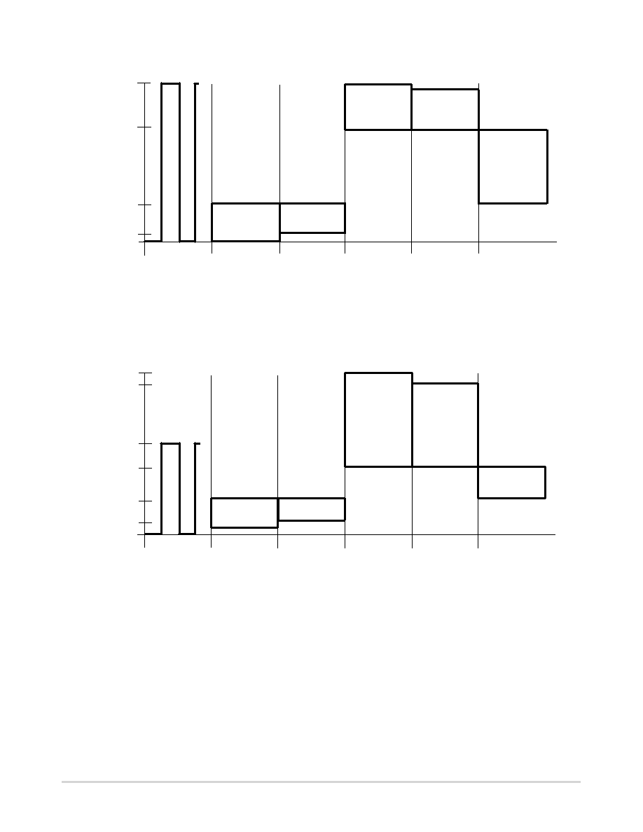
Figure 1–22a. Test Input Signal Levels
Figure 1–22b. Test Input Signal Levels
Test Conditions
Figure 1–22a and 1–22b describe the input signal voltage
levels to be used when testing FACT circuits. The AC test
conditions follow industry convention requiring VIN to
range from 0 V for a logic LOW to 3 V for a logic HIGH for
‘ACT devices and 0 V to VCC for ‘AC devices. The DC
parameters are normally tested with VIN at guaranteed input
levels, that is VIH to VIL (see data tables for details). Care
must be taken to adequately decouple these high
performance parts and to protect the test signals from
electrical noise. In an electrically noisy environment, (e.g.,
a tester and handler not specifically designed for high speed
work), DC input levels may need to be adjusted to increase
the noise margin to allow for the extra noise in the tester
which would not be seen in a system.
Noise immunity testing is performed by raising VIN to the
nominal supply voltage of 5 V then dropping to a level
corresponding to VIH characteristics, and then raising again
to the 5 V level. Noise tests can also be performed on the VIL
characteristics by raising VIN from 0 V to VIL, then
returning to 0 V. Both VIH and VIL noise immunity tests
相关PDF资料 |
PDF描述 |
|---|---|
| MC74AC00M | AC SERIES, QUAD 2-INPUT NAND GATE, PDSO14 |
| MC74AC04MR1 | AC SERIES, HEX 1-INPUT INVERT GATE, PDSO14 |
| MC74AC05MR2 | AC SERIES, HEX 1-INPUT INVERT GATE, PDSO14 |
| MC74ACT05DT | ACT SERIES, HEX 1-INPUT INVERT GATE, PDSO14 |
| MC74AC109N | AC SERIES, DUAL POSITIVE EDGE TRIGGERED J-KBAR FLIP-FLOP, COMPLEMENTARY OUTPUT, PDIP16 |
相关代理商/技术参数 |
参数描述 |
|---|---|
| MC74AC00DTR2 | 功能描述:逻辑门 2-6V Quad 2-Input RoHS:否 制造商:Texas Instruments 产品:OR 逻辑系列:LVC 栅极数量:2 线路数量(输入/输出):2 / 1 高电平输出电流:- 16 mA 低电平输出电流:16 mA 传播延迟时间:3.8 ns 电源电压-最大:5.5 V 电源电压-最小:1.65 V 最大工作温度:+ 125 C 安装风格:SMD/SMT 封装 / 箱体:DCU-8 封装:Reel |
| MC74AC00DTR2G | 功能描述:逻辑门 2-6V Quad 2-Input NAND RoHS:否 制造商:Texas Instruments 产品:OR 逻辑系列:LVC 栅极数量:2 线路数量(输入/输出):2 / 1 高电平输出电流:- 16 mA 低电平输出电流:16 mA 传播延迟时间:3.8 ns 电源电压-最大:5.5 V 电源电压-最小:1.65 V 最大工作温度:+ 125 C 安装风格:SMD/SMT 封装 / 箱体:DCU-8 封装:Reel |
| MC74AC00M | 制造商:Rochester Electronics LLC 功能描述:- Bulk |
| MC74AC00MEL | 功能描述:逻辑门 2-6V Quad 2-Input RoHS:否 制造商:Texas Instruments 产品:OR 逻辑系列:LVC 栅极数量:2 线路数量(输入/输出):2 / 1 高电平输出电流:- 16 mA 低电平输出电流:16 mA 传播延迟时间:3.8 ns 电源电压-最大:5.5 V 电源电压-最小:1.65 V 最大工作温度:+ 125 C 安装风格:SMD/SMT 封装 / 箱体:DCU-8 封装:Reel |
| MC74AC00MELG | 功能描述:逻辑门 2-6V Quad 2-Input NAND RoHS:否 制造商:Texas Instruments 产品:OR 逻辑系列:LVC 栅极数量:2 线路数量(输入/输出):2 / 1 高电平输出电流:- 16 mA 低电平输出电流:16 mA 传播延迟时间:3.8 ns 电源电压-最大:5.5 V 电源电压-最小:1.65 V 最大工作温度:+ 125 C 安装风格:SMD/SMT 封装 / 箱体:DCU-8 封装:Reel |
发布紧急采购,3分钟左右您将得到回复。