- 您现在的位置:买卖IC网 > PDF目录26800 > MC74AC00DT (ON SEMICONDUCTOR) AC SERIES, QUAD 2-INPUT NAND GATE, PDSO14 PDF资料下载
参数资料
| 型号: | MC74AC00DT |
| 厂商: | ON SEMICONDUCTOR |
| 元件分类: | 门电路 |
| 英文描述: | AC SERIES, QUAD 2-INPUT NAND GATE, PDSO14 |
| 封装: | PLASTIC, TSSOP-14 |
| 文件页数: | 30/45页 |
| 文件大小: | 434K |
| 代理商: | MC74AC00DT |
第1页第2页第3页第4页第5页第6页第7页第8页第9页第10页第11页第12页第13页第14页第15页第16页第17页第18页第19页第20页第21页第22页第23页第24页第25页第26页第27页第28页第29页当前第30页第31页第32页第33页第34页第35页第36页第37页第38页第39页第40页第41页第42页第43页第44页第45页
http://onsemi.com
40
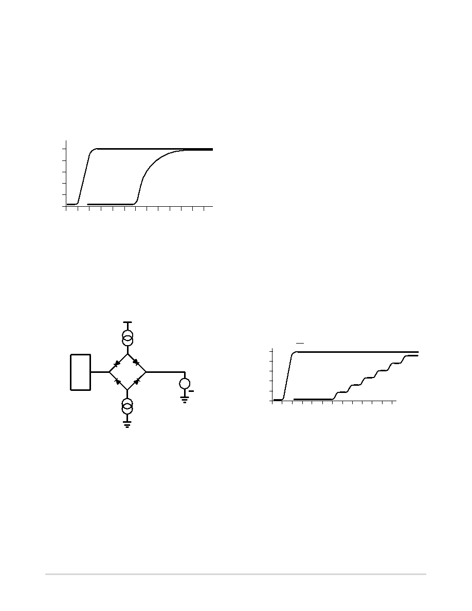
Testing Disable Times of 3-State Outputs in a
Transmission Line Environment
Traditionally, the disable time of a 3-state buffer has been
measured from the 50% point on the disable input, to the
10% or 90% point on the output. On a bench test site, the
output waveform is generated by a load capacitor and a
pull-up/pull-down resistor. This circuit gives an RC
charge/discharge curve as shown below.
5
4
3
2
1
0
1
2
34
5678
9 10
TIME (ns)
VOL
TAGE
(V)
OE
OUTPUT
Figure 1–53. Typical Bench 3-State Waveform
11 12
0
ATE test sites generally are unable to duplicate the bench
test structure. ATE test loads differ because they are usually
programmable and are situated away from the actual device.
A commonly used test load is a Wheatstone bridge. The
following figure illustrates the Wheatstone bridge test
structure when used on the MCT 2000 test-system to
duplicate the bench load.
Figure 1–54. MCT Wheatstone Bridge Test Load
DUT
+
The voltage source provides a pull-up/pull-down voltage
while the current sources provide IOH and IOL. When
devices with slow output slew rates are tested with the ATE
load, the resultant waveforms closely approximate the
bench waveform, and a high degree of correlation can be
achieved. However, when devices with high output slew
rates are tested, different results are observed that make
correlating tester results with bench results more difficult.
This difference is due to the transmission line properties of
the test equipment. Most disable tests are preceded by
establishing a current flow through the output structure.
Typically, these currents will be between 5 mA and 20 mA.
The device is then disabled, and a comparator detects when
the output has risen to the 10% or 90% level.
Consider the situation where the connection between the
device under test (DUT) and the comparator is a
transmission line. Visualize the device output as a switch;
the effect is easier to see. There is current flowing through
the line, and then the switch is opened. At the device end, the
reflection coefficient changes from 0 to 1. This generates a
current edge flowing back down the line equal to the current
flowing in the line prior to the opening of the switch. This
current wave will propagate down the line where it will
encounter the high impedance tester load. This will cause the
wave to be reflected back down the line toward the DUT.
The current wave will continue to reflect in the transmission
line until it reaches the voltage applied to the tester load. At
this point, the current source impedance decreases and it will
dissipate the current. A typical waveshape on a modern ATE
is depicted in Figure 1–51.
Figure 1–55. Typical ATE 3-State Waveform
5
4
3
2
1
0
1 2 3 4 5 6 78 9 10 11 12
TIME(ns)
VOL
TAGE
(V)
OE
OUTPUT
0
相关PDF资料 |
PDF描述 |
|---|---|
| MC74AC00M | AC SERIES, QUAD 2-INPUT NAND GATE, PDSO14 |
| MC74AC04MR1 | AC SERIES, HEX 1-INPUT INVERT GATE, PDSO14 |
| MC74AC05MR2 | AC SERIES, HEX 1-INPUT INVERT GATE, PDSO14 |
| MC74ACT05DT | ACT SERIES, HEX 1-INPUT INVERT GATE, PDSO14 |
| MC74AC109N | AC SERIES, DUAL POSITIVE EDGE TRIGGERED J-KBAR FLIP-FLOP, COMPLEMENTARY OUTPUT, PDIP16 |
相关代理商/技术参数 |
参数描述 |
|---|---|
| MC74AC00DTR2 | 功能描述:逻辑门 2-6V Quad 2-Input RoHS:否 制造商:Texas Instruments 产品:OR 逻辑系列:LVC 栅极数量:2 线路数量(输入/输出):2 / 1 高电平输出电流:- 16 mA 低电平输出电流:16 mA 传播延迟时间:3.8 ns 电源电压-最大:5.5 V 电源电压-最小:1.65 V 最大工作温度:+ 125 C 安装风格:SMD/SMT 封装 / 箱体:DCU-8 封装:Reel |
| MC74AC00DTR2G | 功能描述:逻辑门 2-6V Quad 2-Input NAND RoHS:否 制造商:Texas Instruments 产品:OR 逻辑系列:LVC 栅极数量:2 线路数量(输入/输出):2 / 1 高电平输出电流:- 16 mA 低电平输出电流:16 mA 传播延迟时间:3.8 ns 电源电压-最大:5.5 V 电源电压-最小:1.65 V 最大工作温度:+ 125 C 安装风格:SMD/SMT 封装 / 箱体:DCU-8 封装:Reel |
| MC74AC00M | 制造商:Rochester Electronics LLC 功能描述:- Bulk |
| MC74AC00MEL | 功能描述:逻辑门 2-6V Quad 2-Input RoHS:否 制造商:Texas Instruments 产品:OR 逻辑系列:LVC 栅极数量:2 线路数量(输入/输出):2 / 1 高电平输出电流:- 16 mA 低电平输出电流:16 mA 传播延迟时间:3.8 ns 电源电压-最大:5.5 V 电源电压-最小:1.65 V 最大工作温度:+ 125 C 安装风格:SMD/SMT 封装 / 箱体:DCU-8 封装:Reel |
| MC74AC00MELG | 功能描述:逻辑门 2-6V Quad 2-Input NAND RoHS:否 制造商:Texas Instruments 产品:OR 逻辑系列:LVC 栅极数量:2 线路数量(输入/输出):2 / 1 高电平输出电流:- 16 mA 低电平输出电流:16 mA 传播延迟时间:3.8 ns 电源电压-最大:5.5 V 电源电压-最小:1.65 V 最大工作温度:+ 125 C 安装风格:SMD/SMT 封装 / 箱体:DCU-8 封装:Reel |
发布紧急采购,3分钟左右您将得到回复。