- 您现在的位置:买卖IC网 > PDF目录26800 > MC74AC00DT (ON SEMICONDUCTOR) AC SERIES, QUAD 2-INPUT NAND GATE, PDSO14 PDF资料下载
参数资料
| 型号: | MC74AC00DT |
| 厂商: | ON SEMICONDUCTOR |
| 元件分类: | 门电路 |
| 英文描述: | AC SERIES, QUAD 2-INPUT NAND GATE, PDSO14 |
| 封装: | PLASTIC, TSSOP-14 |
| 文件页数: | 21/45页 |
| 文件大小: | 434K |
| 代理商: | MC74AC00DT |
第1页第2页第3页第4页第5页第6页第7页第8页第9页第10页第11页第12页第13页第14页第15页第16页第17页第18页第19页第20页当前第21页第22页第23页第24页第25页第26页第27页第28页第29页第30页第31页第32页第33页第34页第35页第36页第37页第38页第39页第40页第41页第42页第43页第44页第45页
http://onsemi.com
32
impedance of the driver, the value of the series resistor and
the impedance of the line according to the formula
VW = VCC Zoe/(Zoe + RS + ZS)
The amplitude will be one-half the voltage swing if RS
(the series resistor) plus the output impedance (ZS) of the
driver is equal to the line impedance. The second step of the
waveform is the reflection from the end of the line and will
have an amplitude equal to that of the first step. All devices
on the line will receive a valid level only after the wave has
propagated down the line and returned to the driver.
Therefore, all inputs will see the full voltage swing within
two times the delay of the line.
Parallel Termination
Parallel terminations are not generally recommended for
CMOS circuits due to their power consumption, which can
exceed the power consumption of the logic itself. The power
consumption of parallel terminations is a function of the
resistor value and the duty cycle of the signal. In addition,
parallel termination tends to bias the output levels of the
driver towards either VCC or ground. While this feature is
not desirable for driving CMOS inputs, it can be useful for
driving TTL inputs.
AC Parallel Termination
AC parallel terminations work well for applications
where the delays caused by series terminations are
unacceptable. The effects of AC parallel terminations are
similar to the effects of standard parallel terminations. The
major difference is that the capacitor blocks any DC current
path and helps to reduce power consumption.
Thevenin Termination
Thevenin
terminations
are
also
not
generally
recommended due to their power consumption. Like parallel
termination, a DC path to ground is created by the
terminating resistors. The power consumption of a Thevenin
termination, though, will generally not be a function of the
signal duty cycle. Thevenin terminations are more
applicable for driving CMOS inputs because they do not bias
the output levels as paralleled terminations do. It should be
noted that lines with Thevenin terminations should not be
left floating since this will cause the input levels to float
between VCC or ground, increasing power consumption.
FACT circuits have been designed to drive 50 ohm
transmission lines over the full commercial temperature
range. This is guaranteed by the FACT family’s specified
dynamic drive capability of 86 mA sink and 75 mA source
current. This ensures incident wave switching on 50 ohm
transmission lines and is consistent with the 3 ns rated edge
transition time.
FACT devices also feature balanced output totem pole
structures to allow equal source and sink current capability.
This gives rise to balanced edge rates and equal rise and fall
times. Balanced drive capability and transition times
eliminate both the need to calculate two different delay times
for each signal path and the requirement to correct signal
polarity for the shortest delay time.
FACT product inputs have been created to take full
advantage of high output levels to deliver the maximum
noise immunity to the system designer. VIH and VIL are
specified at 70% and 30% of VCC respectively. The
corresponding output levels, VOH and VOL, are specified to
be within 0.1 V of the rails, of which the output sourcing or
sinking 20
A or less. These noise margins are outlined in
Figure 1–39.
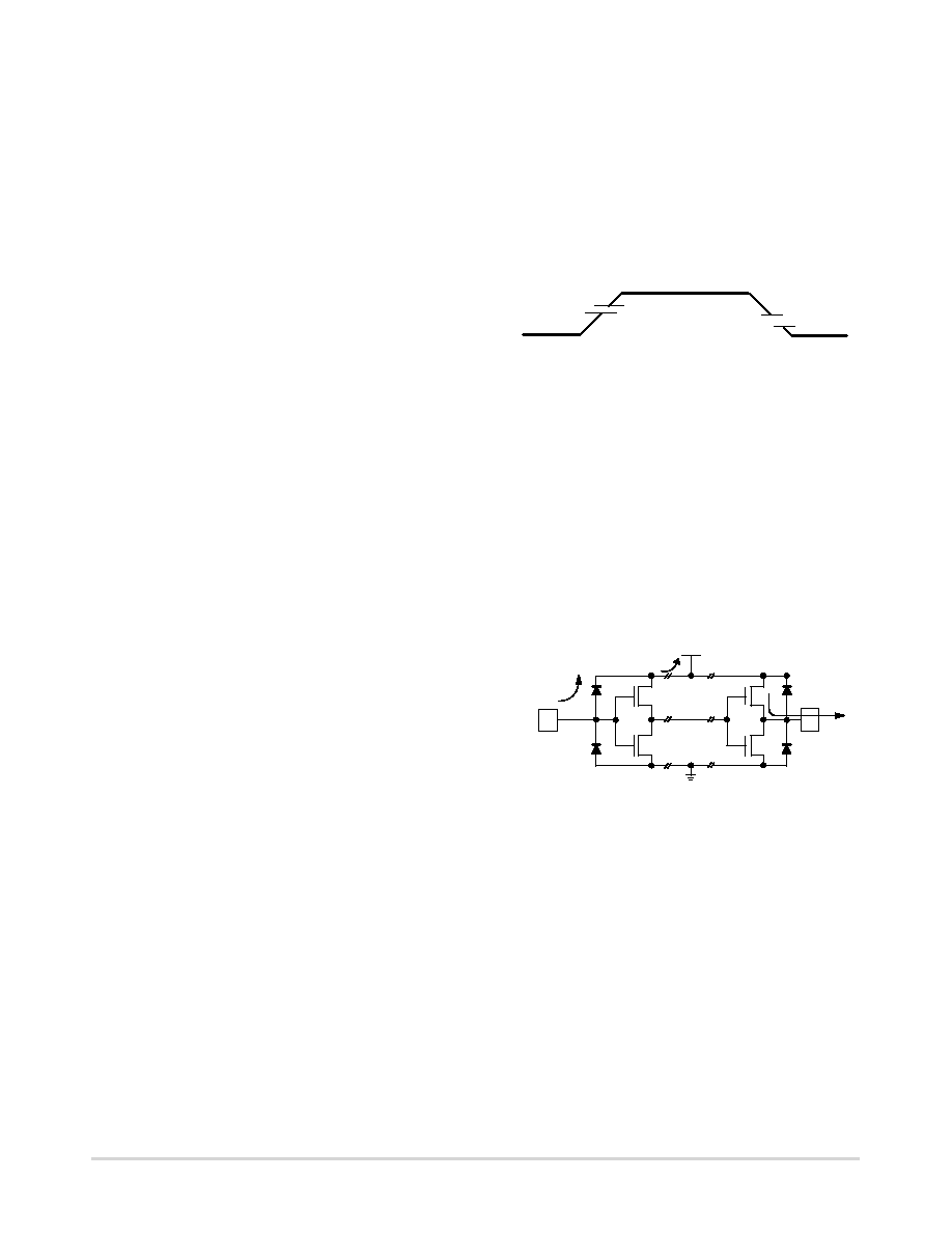
INPUT THRESHOLDS
70%
50%
30%
Figure 1–39. Input Threshold
CMOS Bus Loading
CMOS logic devices have clamp diodes from all inputs
and outputs to VCC and ground. While these diodes increase
system reliability by damping out undershoot and overshoot
noise, they can cause problems if power is lost.
Figure 1–40 exemplifies the situation when power is
removed. Any input driven above the VCC pin will
forward-bias the clamp diode. Current can then flow into the
device, and out VCC or any output that is HIGH. Depending
upon the system, this current, IIN, can be quite high, and may
not allow the bus voltage to reach a valid HIGH state. One
possible solution to eliminate this problem is to place a series
resistor in the line.
Figure 1–40. Noise Effects
IIN
INPUT
ICC
VCC
IOUT
OUTPU
Noise Effects
FACT offers the best noise immunity of any competing
technology available today. With input thresholds specified
at 30% and 70% of VCC and outputs that drive to within 100
mV of the rails, FACT devices offer noise margins
approaching 30% of VCC. At 5 V VCC, FACT’s specified
input and output levels give almost 1.5 V of noise margin for
both ground- and VCC-born noise. With realistic input
thresholds closer to 50% of VCC, the actual margins
approach 2.5 V.
However, even the most advanced technology cannot
alone eliminate noise problems. Good circuit board layout
techniques are essential to take full advantage of the superior
performance of FACT circuits.
相关PDF资料 |
PDF描述 |
|---|---|
| MC74AC00M | AC SERIES, QUAD 2-INPUT NAND GATE, PDSO14 |
| MC74AC04MR1 | AC SERIES, HEX 1-INPUT INVERT GATE, PDSO14 |
| MC74AC05MR2 | AC SERIES, HEX 1-INPUT INVERT GATE, PDSO14 |
| MC74ACT05DT | ACT SERIES, HEX 1-INPUT INVERT GATE, PDSO14 |
| MC74AC109N | AC SERIES, DUAL POSITIVE EDGE TRIGGERED J-KBAR FLIP-FLOP, COMPLEMENTARY OUTPUT, PDIP16 |
相关代理商/技术参数 |
参数描述 |
|---|---|
| MC74AC00DTR2 | 功能描述:逻辑门 2-6V Quad 2-Input RoHS:否 制造商:Texas Instruments 产品:OR 逻辑系列:LVC 栅极数量:2 线路数量(输入/输出):2 / 1 高电平输出电流:- 16 mA 低电平输出电流:16 mA 传播延迟时间:3.8 ns 电源电压-最大:5.5 V 电源电压-最小:1.65 V 最大工作温度:+ 125 C 安装风格:SMD/SMT 封装 / 箱体:DCU-8 封装:Reel |
| MC74AC00DTR2G | 功能描述:逻辑门 2-6V Quad 2-Input NAND RoHS:否 制造商:Texas Instruments 产品:OR 逻辑系列:LVC 栅极数量:2 线路数量(输入/输出):2 / 1 高电平输出电流:- 16 mA 低电平输出电流:16 mA 传播延迟时间:3.8 ns 电源电压-最大:5.5 V 电源电压-最小:1.65 V 最大工作温度:+ 125 C 安装风格:SMD/SMT 封装 / 箱体:DCU-8 封装:Reel |
| MC74AC00M | 制造商:Rochester Electronics LLC 功能描述:- Bulk |
| MC74AC00MEL | 功能描述:逻辑门 2-6V Quad 2-Input RoHS:否 制造商:Texas Instruments 产品:OR 逻辑系列:LVC 栅极数量:2 线路数量(输入/输出):2 / 1 高电平输出电流:- 16 mA 低电平输出电流:16 mA 传播延迟时间:3.8 ns 电源电压-最大:5.5 V 电源电压-最小:1.65 V 最大工作温度:+ 125 C 安装风格:SMD/SMT 封装 / 箱体:DCU-8 封装:Reel |
| MC74AC00MELG | 功能描述:逻辑门 2-6V Quad 2-Input NAND RoHS:否 制造商:Texas Instruments 产品:OR 逻辑系列:LVC 栅极数量:2 线路数量(输入/输出):2 / 1 高电平输出电流:- 16 mA 低电平输出电流:16 mA 传播延迟时间:3.8 ns 电源电压-最大:5.5 V 电源电压-最小:1.65 V 最大工作温度:+ 125 C 安装风格:SMD/SMT 封装 / 箱体:DCU-8 封装:Reel |
发布紧急采购,3分钟左右您将得到回复。