- 您现在的位置:买卖IC网 > PDF目录26800 > MC74AC00DT (ON SEMICONDUCTOR) AC SERIES, QUAD 2-INPUT NAND GATE, PDSO14 PDF资料下载
参数资料
| 型号: | MC74AC00DT |
| 厂商: | ON SEMICONDUCTOR |
| 元件分类: | 门电路 |
| 英文描述: | AC SERIES, QUAD 2-INPUT NAND GATE, PDSO14 |
| 封装: | PLASTIC, TSSOP-14 |
| 文件页数: | 25/45页 |
| 文件大小: | 434K |
| 代理商: | MC74AC00DT |
第1页第2页第3页第4页第5页第6页第7页第8页第9页第10页第11页第12页第13页第14页第15页第16页第17页第18页第19页第20页第21页第22页第23页第24页当前第25页第26页第27页第28页第29页第30页第31页第32页第33页第34页第35页第36页第37页第38页第39页第40页第41页第42页第43页第44页第45页
http://onsemi.com
35
The three waveforms shown in Figure 1–44b, c and d,
depict how ground bounce is generated. The first waveform
shows the voltage (V) across the load as it is switched from
a logic HIGH to a logic LOW. The output slew rate is
dependent upon the characteristics of the output transistor,
the inductors L1 and L3, and CL, the load capacitance. The
second waveform shows the current that is generated as the
capacitor discharges [I = CL dV/dt]. The third waveform
shows the voltage that is induced across the inductance in the
ground lead due to the changing currents [Vgb = –L (dI/dt)].
There are many factors which affect the amplitude of the
ground bounce. Included are:
Number of outputs switching simultaneously: more
outputs results in more ground bounce.
Type of output load: capacitive loads generate two to
three times more ground bounce than typical system
traces. Increasing the capacitive load to approximately
60–70 pF increases ground bounce. Beyond 70 pF,
ground bounce drops off due to the filtering effect of
the load. Moving the load away from the output reduces
the ground bounce.
Location of the output pin: outputs closer to the ground
pin exhibit less ground bounce than those further away.
Voltage: lowering VCC reduces ground bounce.
Test fixtures: standard test fixtures generate 30 to 50%
more ground bounce than a typical system since they
use capacitive loads which both increase the AC load
and form LCR tank circuits that oscillate.
Ground bounce produces several symptoms:
Altered device states. FACT logic does not exhibit this
symptom.
Propagation delay degradation. FACT devices are
characterized not to degrade more than 250 ps per
additional output switching.
Undershoot on active outputs. The worst-case
undershoot will be approximately equal to the
worst-case quiet output noise.
Quiet output noise. FACT logic’s worst-case quiet
output noise has been measured to be approximately
500-1100 mV in actual system applications.
Observing either one of the following rules is sufficient to
avoid running into any of the problems associated with
ground bounce:
First, use caution when driving asynchronous
TTL-level inputs from CMOS octal outputs, or
Second, use caution when running control lines (set,
reset,
load,
clock,
chip
select)
which
are
glitch-sensitive through the same devices that drive
data or address lines.
When it is not possible to avoid the above conditions,
there are simple precautions available which can minimize
ground bounce noise. These are:
Locate these outputs as close to the ground pin as
possible.
Use the lowest VCC possible or separate the power
supplies.
Use board design practices which reduce any additive
noise sources, such as crosstalk, reflections, etc.
Design Rules
The set of design rules listed below are recommended to
ensure reliable system operation by providing the optimum
power supply connection to the devices. Most designers will
recognize these guidelines as those they have employed with
advanced bipolar logic families.
Use multi-layer boards with VCC and ground planes,
with the device power pins soldered directly to the
planes to insure the lowest power line impedances
possible.
Use decoupling capacitors for every device, usually 0. 1
F should be adequate. These capacitors should be
located as close to the ground pin as possible.
Do not use sockets or wirewrap boards whenever
possible.
Do not connect capacitors from the outputs directly to
ground.
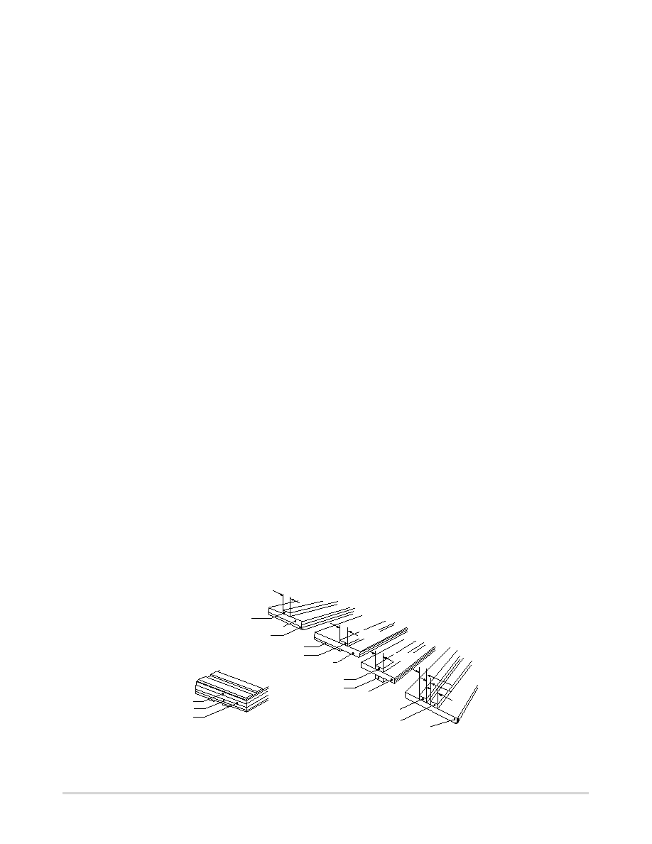
Figure 1–45. Power Distribution Impedances
VCC
1/16″ GLASSEPOXY
GROUND PLANE
GND
D) 100 VCC
IMPEDANCE
GND
.032
EPOXY GLASS
E) 2.0 VCC
IMPEDANCE
VCC
1/16" BOARD
B) 100 VCC
IMPEDANCE
VCC
GND
1/16″ BOARD
C) 68 VCC
IMPEDANCE
1/16″ BOARD
VCC
GND
0.1″
0.04"
A) 50 VCC
IMPEDANCE
相关PDF资料 |
PDF描述 |
|---|---|
| MC74AC00M | AC SERIES, QUAD 2-INPUT NAND GATE, PDSO14 |
| MC74AC04MR1 | AC SERIES, HEX 1-INPUT INVERT GATE, PDSO14 |
| MC74AC05MR2 | AC SERIES, HEX 1-INPUT INVERT GATE, PDSO14 |
| MC74ACT05DT | ACT SERIES, HEX 1-INPUT INVERT GATE, PDSO14 |
| MC74AC109N | AC SERIES, DUAL POSITIVE EDGE TRIGGERED J-KBAR FLIP-FLOP, COMPLEMENTARY OUTPUT, PDIP16 |
相关代理商/技术参数 |
参数描述 |
|---|---|
| MC74AC00DTR2 | 功能描述:逻辑门 2-6V Quad 2-Input RoHS:否 制造商:Texas Instruments 产品:OR 逻辑系列:LVC 栅极数量:2 线路数量(输入/输出):2 / 1 高电平输出电流:- 16 mA 低电平输出电流:16 mA 传播延迟时间:3.8 ns 电源电压-最大:5.5 V 电源电压-最小:1.65 V 最大工作温度:+ 125 C 安装风格:SMD/SMT 封装 / 箱体:DCU-8 封装:Reel |
| MC74AC00DTR2G | 功能描述:逻辑门 2-6V Quad 2-Input NAND RoHS:否 制造商:Texas Instruments 产品:OR 逻辑系列:LVC 栅极数量:2 线路数量(输入/输出):2 / 1 高电平输出电流:- 16 mA 低电平输出电流:16 mA 传播延迟时间:3.8 ns 电源电压-最大:5.5 V 电源电压-最小:1.65 V 最大工作温度:+ 125 C 安装风格:SMD/SMT 封装 / 箱体:DCU-8 封装:Reel |
| MC74AC00M | 制造商:Rochester Electronics LLC 功能描述:- Bulk |
| MC74AC00MEL | 功能描述:逻辑门 2-6V Quad 2-Input RoHS:否 制造商:Texas Instruments 产品:OR 逻辑系列:LVC 栅极数量:2 线路数量(输入/输出):2 / 1 高电平输出电流:- 16 mA 低电平输出电流:16 mA 传播延迟时间:3.8 ns 电源电压-最大:5.5 V 电源电压-最小:1.65 V 最大工作温度:+ 125 C 安装风格:SMD/SMT 封装 / 箱体:DCU-8 封装:Reel |
| MC74AC00MELG | 功能描述:逻辑门 2-6V Quad 2-Input NAND RoHS:否 制造商:Texas Instruments 产品:OR 逻辑系列:LVC 栅极数量:2 线路数量(输入/输出):2 / 1 高电平输出电流:- 16 mA 低电平输出电流:16 mA 传播延迟时间:3.8 ns 电源电压-最大:5.5 V 电源电压-最小:1.65 V 最大工作温度:+ 125 C 安装风格:SMD/SMT 封装 / 箱体:DCU-8 封装:Reel |
发布紧急采购,3分钟左右您将得到回复。