- 您现在的位置:买卖IC网 > PDF目录26800 > MC74AC00DT (ON SEMICONDUCTOR) AC SERIES, QUAD 2-INPUT NAND GATE, PDSO14 PDF资料下载
参数资料
| 型号: | MC74AC00DT |
| 厂商: | ON SEMICONDUCTOR |
| 元件分类: | 门电路 |
| 英文描述: | AC SERIES, QUAD 2-INPUT NAND GATE, PDSO14 |
| 封装: | PLASTIC, TSSOP-14 |
| 文件页数: | 26/45页 |
| 文件大小: | 434K |
| 代理商: | MC74AC00DT |
第1页第2页第3页第4页第5页第6页第7页第8页第9页第10页第11页第12页第13页第14页第15页第16页第17页第18页第19页第20页第21页第22页第23页第24页第25页当前第26页第27页第28页第29页第30页第31页第32页第33页第34页第35页第36页第37页第38页第39页第40页第41页第42页第43页第44页第45页
http://onsemi.com
36
Decoupling Requirements
ON Semiconductor Advanced CMOS, as with other high-
performance, high-drive logic families, has special
decoupling and printed circuit board layout requirements.
Adhering to these requirements will ensure the maximum
advantages are gained with FACT products.
Local high frequency decoupling is required to supply
power to the chip when it is transitioning from a LOW to a
HIGH value. This power is necessary to charge the load
capacitance or drive a line impedance. Figure 1–45 displays
various VCC and ground layout schemes along with
associated impedances.
For most power distribution networks, the typical
impedance is between 50 and 100 ohms. This impedance
appears in series with the load impedance and will cause a
droop in the VCC at the part. This limits the available voltage
swing at the local node, unless some form of decoupling is
used. This drooping of rails will cause the rise and fall times
to become elongated. Consider the example described in
Figure 1–46 to calculate the amount of decoupling
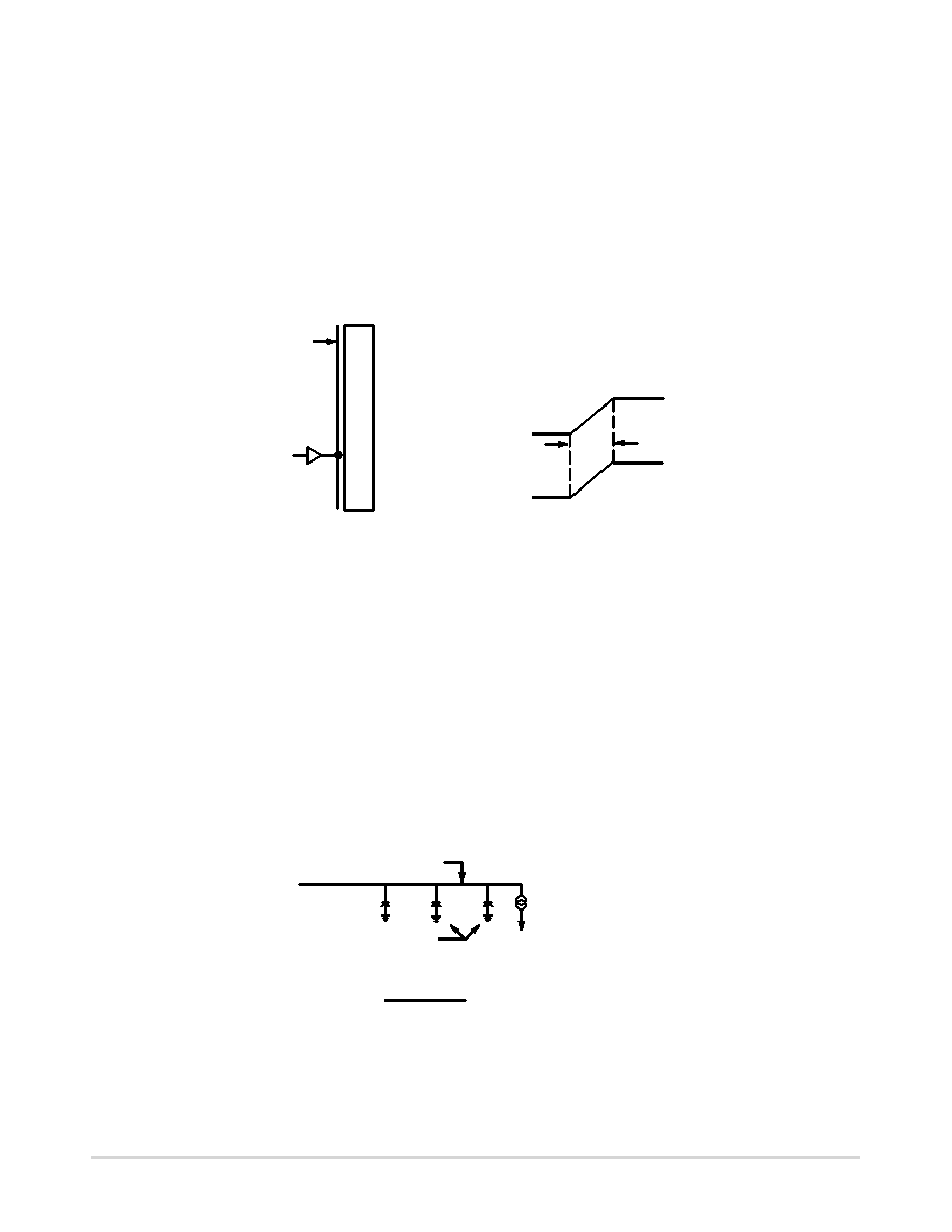
necessary. This circuit utilizes an ‘AC240 driving a 100 ohm
bus from a point somewhere in the middle.
DATA BUS
100
BUFFER
1 OF 8
100 V
GROUND
PLANE
VOUT
0.1 V
IOH
0
4.9 V
4.0 ns
94 mA
Worst-Case Octal Drain = 8
× 94 mA = 0.75 Amp.
Figure 1–46. Octal Buffer Driving a 100 Ohm Bus
Buffer Output Sees Net 50
Load.
50
Load Line on IOH–VOH Characteristic
Shows Low-to-High Step of Approx. 4.8 V
Being in the middle of the bus, the driver will see two 100
ohm loads in parallel, or an effective impedance of 50 ohms.
To switch the line from rail to rail, a drive of 94 mA is
needed; more than 750 mA will be required if all eight lines
switch at once. This instantaneous current requirement will
generate a voltage across the impedance of the power lines,
causing the actual VCC at the chip to droop. This droop limits
the voltage swing available to the driver. The net effect of the
voltage droop will lengthen device rise and fall times and
slow system operation. A local decoupling capacitor is
required to act as a low impedance supply for the driver chip
during high current conditions. It will maintain the voltage
within acceptable limits and keep rise and fall times to a
minimum. The necessary values for decoupling capacitors
can be calculated with the formula given in Figure 1–47.
In this example, if the VCC droop is to be kept below 0.1
V and the edge rate equals 4 ns, a 0.03
F capacitor is
needed.
It is good practice to distribute decoupling capacitors
evenly through the logic, placing one capacitor for every
package.
Capacitor Types
Decoupling capacitors need to be of the high K ceramic
type with low equivalent series resistance (ESR), consisting
primarily of series inductance and series resistance.
Capacitors using 5ZU dielectric have suitable properties and
make a good choice for decoupling capacitors; they offer
minimum cost and effective performance.
Figure 1–47. Formula for Calculating Decoupling Capacitors
VCC BUS
VCC
ZCC
CB
BYPASS CAPACITORS
SPECIFY VCC DROOP = 0.1 V MAX.
I = 0.75 A
Q = CV
I = CV/t
C = It/V
t = 4 × 10 -9
C = 0.750
× 4 × 10-9
0.1
= 30 × 10-9 = 0.030 F
SELECT CB ≥ 0.047 F
Place one decoupling capacitor adjacent to each package driving any transmission line and distribute others evenly throughout the logic.
相关PDF资料 |
PDF描述 |
|---|---|
| MC74AC00M | AC SERIES, QUAD 2-INPUT NAND GATE, PDSO14 |
| MC74AC04MR1 | AC SERIES, HEX 1-INPUT INVERT GATE, PDSO14 |
| MC74AC05MR2 | AC SERIES, HEX 1-INPUT INVERT GATE, PDSO14 |
| MC74ACT05DT | ACT SERIES, HEX 1-INPUT INVERT GATE, PDSO14 |
| MC74AC109N | AC SERIES, DUAL POSITIVE EDGE TRIGGERED J-KBAR FLIP-FLOP, COMPLEMENTARY OUTPUT, PDIP16 |
相关代理商/技术参数 |
参数描述 |
|---|---|
| MC74AC00DTR2 | 功能描述:逻辑门 2-6V Quad 2-Input RoHS:否 制造商:Texas Instruments 产品:OR 逻辑系列:LVC 栅极数量:2 线路数量(输入/输出):2 / 1 高电平输出电流:- 16 mA 低电平输出电流:16 mA 传播延迟时间:3.8 ns 电源电压-最大:5.5 V 电源电压-最小:1.65 V 最大工作温度:+ 125 C 安装风格:SMD/SMT 封装 / 箱体:DCU-8 封装:Reel |
| MC74AC00DTR2G | 功能描述:逻辑门 2-6V Quad 2-Input NAND RoHS:否 制造商:Texas Instruments 产品:OR 逻辑系列:LVC 栅极数量:2 线路数量(输入/输出):2 / 1 高电平输出电流:- 16 mA 低电平输出电流:16 mA 传播延迟时间:3.8 ns 电源电压-最大:5.5 V 电源电压-最小:1.65 V 最大工作温度:+ 125 C 安装风格:SMD/SMT 封装 / 箱体:DCU-8 封装:Reel |
| MC74AC00M | 制造商:Rochester Electronics LLC 功能描述:- Bulk |
| MC74AC00MEL | 功能描述:逻辑门 2-6V Quad 2-Input RoHS:否 制造商:Texas Instruments 产品:OR 逻辑系列:LVC 栅极数量:2 线路数量(输入/输出):2 / 1 高电平输出电流:- 16 mA 低电平输出电流:16 mA 传播延迟时间:3.8 ns 电源电压-最大:5.5 V 电源电压-最小:1.65 V 最大工作温度:+ 125 C 安装风格:SMD/SMT 封装 / 箱体:DCU-8 封装:Reel |
| MC74AC00MELG | 功能描述:逻辑门 2-6V Quad 2-Input NAND RoHS:否 制造商:Texas Instruments 产品:OR 逻辑系列:LVC 栅极数量:2 线路数量(输入/输出):2 / 1 高电平输出电流:- 16 mA 低电平输出电流:16 mA 传播延迟时间:3.8 ns 电源电压-最大:5.5 V 电源电压-最小:1.65 V 最大工作温度:+ 125 C 安装风格:SMD/SMT 封装 / 箱体:DCU-8 封装:Reel |
发布紧急采购,3分钟左右您将得到回复。