- 您现在的位置:买卖IC网 > PDF目录26800 > MC74AC00DT (ON SEMICONDUCTOR) AC SERIES, QUAD 2-INPUT NAND GATE, PDSO14 PDF资料下载
参数资料
| 型号: | MC74AC00DT |
| 厂商: | ON SEMICONDUCTOR |
| 元件分类: | 门电路 |
| 英文描述: | AC SERIES, QUAD 2-INPUT NAND GATE, PDSO14 |
| 封装: | PLASTIC, TSSOP-14 |
| 文件页数: | 17/45页 |
| 文件大小: | 434K |
| 代理商: | MC74AC00DT |
第1页第2页第3页第4页第5页第6页第7页第8页第9页第10页第11页第12页第13页第14页第15页第16页当前第17页第18页第19页第20页第21页第22页第23页第24页第25页第26页第27页第28页第29页第30页第31页第32页第33页第34页第35页第36页第37页第38页第39页第40页第41页第42页第43页第44页第45页
http://onsemi.com
28
Thermal Resistance In Still Air
Package Description
No
Body
Die
Die Area
Flag Area
θJC (°C/Watt)
No.
Leads
Body
Style
Body
Material
Body
W
× L
Die
Bonds
Die Area
(Sq. Mils)
Flag Area
(Sg. Mils)
Avg.
Max.
14
DIL
Epoxy
1/4
″× 3/4″
Epoxy
4096
6,400
38
61
16
DIL
Epoxy
1/4
″× 3/4″
Epoxy
4096
12,100
34
54
20
DIL
Epoxy
0.35
″× 0.35″
Epoxy
4096
14,400
N/A
NOTES:
1. All plastic packages use copper lead frames.
2. Body style DIL is “Dual-In-Line.”
3. Standard Mounting Method: Dual-In-Line Socket or P/C board with no contact between bottom of package and socket or P/C board.
Figure 1–28. Thermal Resistance Values for Standard I/C Packages
For applications where the case is held at essentially a
fixed temperature by mounting on a large or temperature-
controlled heat sink, the estimated junction temperature is
calculated by:
TJ = TC + PD(θJC)(3)
where TC = maximum case temperature and the other
parameters are as previously defined.
The maximum and average
θJC resistance values for
standard IC packages are given in Figure 1–28. In
Figure 1–29, this basic data is converted into graphs
showing the maximum power dissipation allowable at
various ambient temperatures (still air) for circuits mounted
in the different packages, taking into account the maximum
permissible operating junction temperature for long term
life (
≥ 100,000 hours for ceramic packages).
2000
1750
1500
1250
1000
750
500
250
0
25
50
75
100
125
150
175
200
140
24 LEAD
16 LEAD
14 LEAD
8 LEAD
TA, AMBIENT TEMPERATURE - STILL AIR (°C)
MAXIMUM
ALLOWED
POWER
DISSIP
ATION
(mW/P
k
Figure 1–29. Ambient Temperature Derating Curves
(Plastic Dual-In-Line Package Test Environment)
Air Flow
The effect of air flow over the packages on
θJA (due to a
decrease in
θCA) reduces the temperature rise of the
package, therefore permitting a corresponding increase in
power dissipation without exceeding the maximum
permissible operating junction temperature.
Even though different device types mounted on a printed
circuit board may each have different power dissipations, all
will have the same input and output levels provided that each
is subject to identical air flow and the same ambient air
temperature. This eases design, since the only change in
levels between devices is due to the increase in ambient
temperatures as the air passes over the devices, or
differences in ambient temperature between two devices.
The majority of users employ some form of air-flow
cooling. As air passes over each device on a printed circuit
board, it absorbs heat from each package. This heat gradient
from the first package to the last package is a function of the
air flow rate and individual package dissipations.
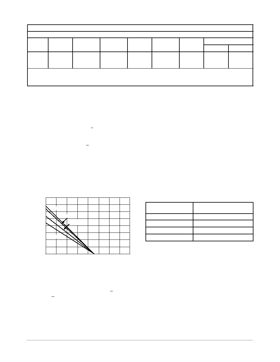
Figure 1–30 provides gradient data at power levels of 200
mW, 250 mW, 300 mW, and 400 mW with an air flow rate
of 500 Ifpm. These figures show the proportionate increase
in the junction temperature of each dual in-line package as
the air passes over each device. For higher rates of air flow
the change in junction temperature from package to package
down the airstream will be lower due to greater cooling.
Power Dissipation
(mW)
Junction Temperature Gradient
(
°C/Package)
200
0.4
250
0.5
300
0.63
400
0.88
Devices mounted on 0.062
″ PC board with Z axis spacing of 0.5″.
Air flow is 500 lfpm along the Z axis.
Figure 1–30. Thermal Gradient of Junction
Temperature (16-Pin Dual-In-Line Package)
Optimizing The Long Term Reliability of
Plastic Packages
Todays plastic integrated circuit packages are as reliable
as ceramic packages under most environmental conditions.
However when the ultimate in system reliability is required,
thermal management must be considered as a prime system
design goal.
Modern plastic package assembly technology utilizes
gold wire bonded to aluminum bonding pads throughout the
electronics industry. When exposed to high temperatures for
protracted periods of time an intermetallic compound can
相关PDF资料 |
PDF描述 |
|---|---|
| MC74AC00M | AC SERIES, QUAD 2-INPUT NAND GATE, PDSO14 |
| MC74AC04MR1 | AC SERIES, HEX 1-INPUT INVERT GATE, PDSO14 |
| MC74AC05MR2 | AC SERIES, HEX 1-INPUT INVERT GATE, PDSO14 |
| MC74ACT05DT | ACT SERIES, HEX 1-INPUT INVERT GATE, PDSO14 |
| MC74AC109N | AC SERIES, DUAL POSITIVE EDGE TRIGGERED J-KBAR FLIP-FLOP, COMPLEMENTARY OUTPUT, PDIP16 |
相关代理商/技术参数 |
参数描述 |
|---|---|
| MC74AC00DTR2 | 功能描述:逻辑门 2-6V Quad 2-Input RoHS:否 制造商:Texas Instruments 产品:OR 逻辑系列:LVC 栅极数量:2 线路数量(输入/输出):2 / 1 高电平输出电流:- 16 mA 低电平输出电流:16 mA 传播延迟时间:3.8 ns 电源电压-最大:5.5 V 电源电压-最小:1.65 V 最大工作温度:+ 125 C 安装风格:SMD/SMT 封装 / 箱体:DCU-8 封装:Reel |
| MC74AC00DTR2G | 功能描述:逻辑门 2-6V Quad 2-Input NAND RoHS:否 制造商:Texas Instruments 产品:OR 逻辑系列:LVC 栅极数量:2 线路数量(输入/输出):2 / 1 高电平输出电流:- 16 mA 低电平输出电流:16 mA 传播延迟时间:3.8 ns 电源电压-最大:5.5 V 电源电压-最小:1.65 V 最大工作温度:+ 125 C 安装风格:SMD/SMT 封装 / 箱体:DCU-8 封装:Reel |
| MC74AC00M | 制造商:Rochester Electronics LLC 功能描述:- Bulk |
| MC74AC00MEL | 功能描述:逻辑门 2-6V Quad 2-Input RoHS:否 制造商:Texas Instruments 产品:OR 逻辑系列:LVC 栅极数量:2 线路数量(输入/输出):2 / 1 高电平输出电流:- 16 mA 低电平输出电流:16 mA 传播延迟时间:3.8 ns 电源电压-最大:5.5 V 电源电压-最小:1.65 V 最大工作温度:+ 125 C 安装风格:SMD/SMT 封装 / 箱体:DCU-8 封装:Reel |
| MC74AC00MELG | 功能描述:逻辑门 2-6V Quad 2-Input NAND RoHS:否 制造商:Texas Instruments 产品:OR 逻辑系列:LVC 栅极数量:2 线路数量(输入/输出):2 / 1 高电平输出电流:- 16 mA 低电平输出电流:16 mA 传播延迟时间:3.8 ns 电源电压-最大:5.5 V 电源电压-最小:1.65 V 最大工作温度:+ 125 C 安装风格:SMD/SMT 封装 / 箱体:DCU-8 封装:Reel |
发布紧急采购,3分钟左右您将得到回复。