- 您现在的位置:买卖IC网 > PDF目录26800 > MC74AC00DT (ON SEMICONDUCTOR) AC SERIES, QUAD 2-INPUT NAND GATE, PDSO14 PDF资料下载
参数资料
| 型号: | MC74AC00DT |
| 厂商: | ON SEMICONDUCTOR |
| 元件分类: | 门电路 |
| 英文描述: | AC SERIES, QUAD 2-INPUT NAND GATE, PDSO14 |
| 封装: | PLASTIC, TSSOP-14 |
| 文件页数: | 8/45页 |
| 文件大小: | 434K |
| 代理商: | MC74AC00DT |
第1页第2页第3页第4页第5页第6页第7页当前第8页第9页第10页第11页第12页第13页第14页第15页第16页第17页第18页第19页第20页第21页第22页第23页第24页第25页第26页第27页第28页第29页第30页第31页第32页第33页第34页第35页第36页第37页第38页第39页第40页第41页第42页第43页第44页第45页
http://onsemi.com
20
Section 3 – Ratings, Specifications and Waveforms
Specifying FACT Devices
Traditionally, when a semiconductor manufacturer
completed a new device for introduction, specifications
were based on the characterization of just a few parts. While
these specifications were appealing to the designer, they
were often too tight and, over time, the IC manufacturers had
difficulty producing devices to the original specs. This
forced the manufacturer to relax circuit specifications to
reflect the actual performance of the device.
As a result, designers were required to review system
designs to ensure the system would remain reliable with the
new specifications. ON Semiconductor realized and
understood the problems associated with characterizing
devices too aggressively.
To provide more realistic and manufacturable specs, ON
Semiconductor devised a systematic and thorough process
to generate specifications. Devices are selected from
multiple wafer lots to ensure process variations are taken
into account. In addition, the process parameters are
measured and compared to the known process limits.
This method of characterizing parts more accurately
represents the product across time, voltage, temperature and
process rather than portraying the fastest possible device.
FACT
circuits
are
therefore
guaranteed
to
be
manufacturable over time without the need to respecify
timing.
These specification guidelines allow designers to design
systems more efficiently since the devices used will behave
as documented. Unspecified guardbands no longer need to
be added by the designer to ensure system reliability.
Power Dissipation – Test Philosophy
In an effort to reduce confusion about measuring CPD, a
JEDEC standard test procedure (per JEDEC, Appendix E)
has been adopted which specifies the test setup for each type
of device. This allows a device to be exercised in a consistent
manner for the purpose of specification comparison. All
device measurements are made with VCC = 5 V at 25°C, with
3-state outputs both enabled and disabled.
Gates – Switch one input. Bias the remaining inputs such
that the output switches.
Latches – Switch the Enable and D inputs such that the latch
toggles.
Flip-Flops – Switch the clock pin while changing D (or bias
J and K) such that the output(s) change each clock cycle. For
parts with a common clock, exercise only one flip-flop.
Decoders – Switch one address pin which changes two
outputs.
Multiplexers
–
Switch
one
address
pin
with
the
corresponding data inputs at opposite logic levels so that the
output switches.
Counters – Switch the clock pin with other inputs biased
such that the device counts.
Shift Registers – Switch the clock pin with other inputs
biased such that the device counts.
Transceivers – Switch one data input. For bidirectional
devices enable only one direction.
Parity Generator – Switch one input.
Priority Encoders – Switch the lowest priority input.
Load Capacitance – Each output which is switching should
be loaded with the standard 50 pF.
If the device is tested at a high enough frequency, the static
supply current can be ignored. Thus at 1 MHz, the following
formula can be used to calculate CPD:
CPD = ICC/(VCC) (1 × 10⁶) – Equivalent Load Capacitance
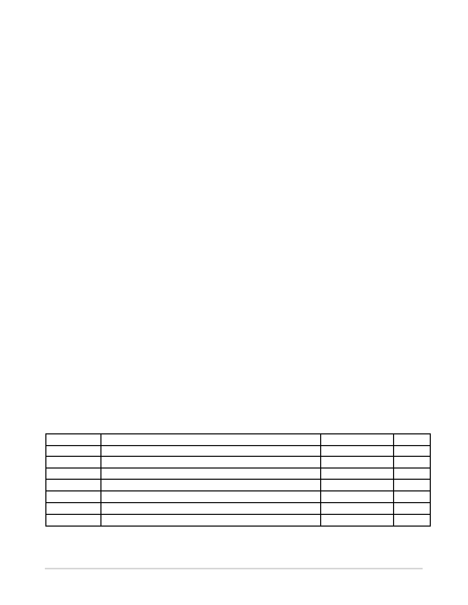
Ratings and Specifications
Symbol
Parameter
Value
Unit
VCC
DC Supply Voltage (Referenced to GND)
–0.5 to +7.0
V
Vin
DC Input Voltage (Referenced to GND)
–0.5 to VCC +0.5
V
Vout
DC Output Voltage (Referenced to GND)
–0.5 to VCC +0.5
V
Iin
DC Input Current, per Pin
±20
mA
Iout
DC Output Source/Sink Current, per Pin
±50
mA
ICC
DC VCC or GND Current per Output Pin
±50
mA
Tstg
Storage Temperature
–65 to +150
°C
1Absolute maximum ratings are those values beyond which damage to the device may occur. Obviously the databook specifications should
be met, without exception to ensure that the system design is reliable over its power supply, temperature, output/input loading variables.
ON Semiconductor does not recommend operation of FACT circuits outside databook specifications.
相关PDF资料 |
PDF描述 |
|---|---|
| MC74AC00M | AC SERIES, QUAD 2-INPUT NAND GATE, PDSO14 |
| MC74AC04MR1 | AC SERIES, HEX 1-INPUT INVERT GATE, PDSO14 |
| MC74AC05MR2 | AC SERIES, HEX 1-INPUT INVERT GATE, PDSO14 |
| MC74ACT05DT | ACT SERIES, HEX 1-INPUT INVERT GATE, PDSO14 |
| MC74AC109N | AC SERIES, DUAL POSITIVE EDGE TRIGGERED J-KBAR FLIP-FLOP, COMPLEMENTARY OUTPUT, PDIP16 |
相关代理商/技术参数 |
参数描述 |
|---|---|
| MC74AC00DTR2 | 功能描述:逻辑门 2-6V Quad 2-Input RoHS:否 制造商:Texas Instruments 产品:OR 逻辑系列:LVC 栅极数量:2 线路数量(输入/输出):2 / 1 高电平输出电流:- 16 mA 低电平输出电流:16 mA 传播延迟时间:3.8 ns 电源电压-最大:5.5 V 电源电压-最小:1.65 V 最大工作温度:+ 125 C 安装风格:SMD/SMT 封装 / 箱体:DCU-8 封装:Reel |
| MC74AC00DTR2G | 功能描述:逻辑门 2-6V Quad 2-Input NAND RoHS:否 制造商:Texas Instruments 产品:OR 逻辑系列:LVC 栅极数量:2 线路数量(输入/输出):2 / 1 高电平输出电流:- 16 mA 低电平输出电流:16 mA 传播延迟时间:3.8 ns 电源电压-最大:5.5 V 电源电压-最小:1.65 V 最大工作温度:+ 125 C 安装风格:SMD/SMT 封装 / 箱体:DCU-8 封装:Reel |
| MC74AC00M | 制造商:Rochester Electronics LLC 功能描述:- Bulk |
| MC74AC00MEL | 功能描述:逻辑门 2-6V Quad 2-Input RoHS:否 制造商:Texas Instruments 产品:OR 逻辑系列:LVC 栅极数量:2 线路数量(输入/输出):2 / 1 高电平输出电流:- 16 mA 低电平输出电流:16 mA 传播延迟时间:3.8 ns 电源电压-最大:5.5 V 电源电压-最小:1.65 V 最大工作温度:+ 125 C 安装风格:SMD/SMT 封装 / 箱体:DCU-8 封装:Reel |
| MC74AC00MELG | 功能描述:逻辑门 2-6V Quad 2-Input NAND RoHS:否 制造商:Texas Instruments 产品:OR 逻辑系列:LVC 栅极数量:2 线路数量(输入/输出):2 / 1 高电平输出电流:- 16 mA 低电平输出电流:16 mA 传播延迟时间:3.8 ns 电源电压-最大:5.5 V 电源电压-最小:1.65 V 最大工作温度:+ 125 C 安装风格:SMD/SMT 封装 / 箱体:DCU-8 封装:Reel |
发布紧急采购,3分钟左右您将得到回复。