参数资料
| 型号: | MCP669T-E/ML |
| 厂商: | Microchip Technology |
| 文件页数: | 15/68页 |
| 文件大小: | 0K |
| 描述: | IC OPAMP QUAD 60MHZ 16QFN |
| 标准包装: | 3,300 |
| 放大器类型: | 通用 |
| 电路数: | 4 |
| 输出类型: | 满摆幅 |
| 转换速率: | 32 V/µs |
| 增益带宽积: | 60MHz |
| 电流 - 输入偏压: | 6pA |
| 电压 - 输入偏移: | 1800µV |
| 电流 - 电源: | 6mA |
| 电流 - 输出 / 通道: | 80mA |
| 电压 - 电源,单路/双路(±): | 2.5 V ~ 5.5 V,±1.25 V ~ 2.75 V |
| 工作温度: | -40°C ~ 125°C |
| 安装类型: | 表面贴装 |
| 封装/外壳: | 16-VQFN 裸露焊盘 |
| 供应商设备封装: | 16-QFN(4x4) |
| 包装: | 带卷 (TR) |
第1页第2页第3页第4页第5页第6页第7页第8页第9页第10页第11页第12页第13页第14页当前第15页第16页第17页第18页第19页第20页第21页第22页第23页第24页第25页第26页第27页第28页第29页第30页第31页第32页第33页第34页第35页第36页第37页第38页第39页第40页第41页第42页第43页第44页第45页第46页第47页第48页第49页第50页第51页第52页第53页第54页第55页第56页第57页第58页第59页第60页第61页第62页第63页第64页第65页第66页第67页第68页
MCP660/1/2/3/4/5/9
DS22194D-page 22
2009-2012 Microchip Technology Inc.
4.2
Rail-to-Rail Output
4.2.1
MAXIMUM OUTPUT VOLTAGE
The Maximum Output Voltage (see Figure 2-16 and
Figure 2-17) describes the output range for a given
load. For example, the output voltage swings to within
50 mV of the negative rail with a 1 k
load tied to
VDD/2.
4.2.2
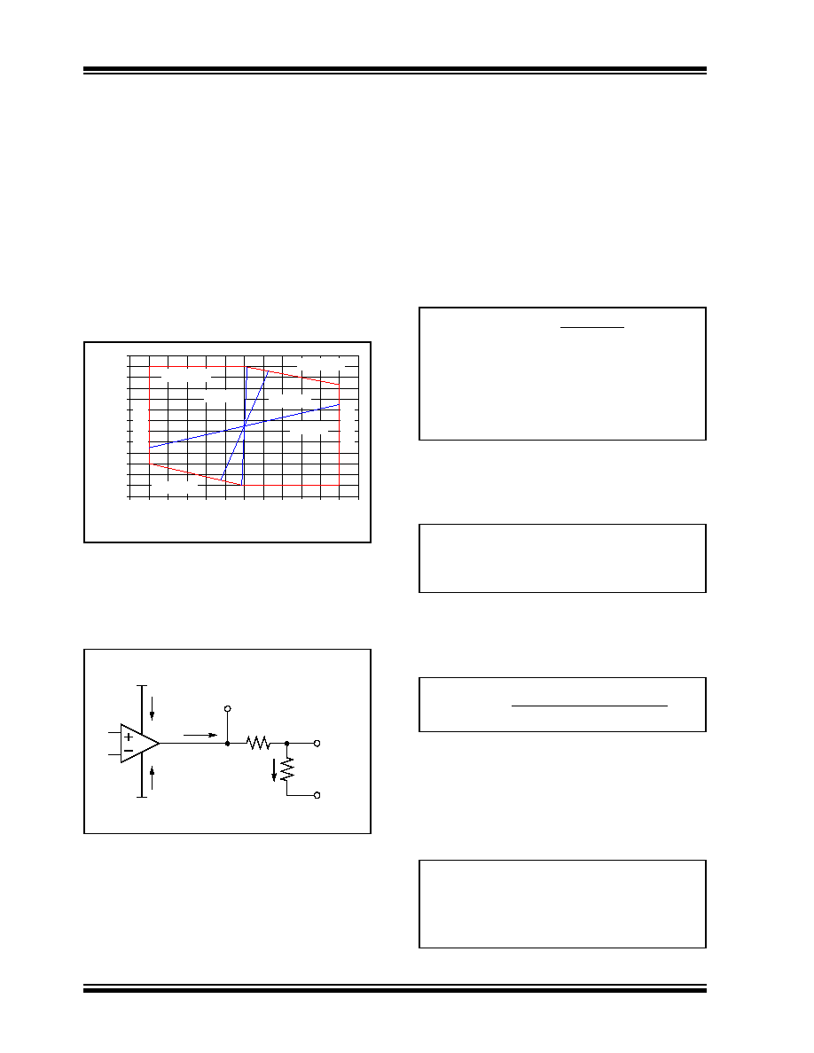
OUTPUT CURRENT
Figure 4-4 shows the possible combinations of output
voltage (VOUT) and output current (IOUT), when VDD =
5.5V.
IOUT is positive when it flows out of the op amp into the
external circuit.
FIGURE 4-4:
Output Current.
4.2.3
POWER DISSIPATION
Since the output short circuit current (ISC) is specified
at ±90 mA (typical), these op amps are capable of both
delivering and dissipating significant power.
FIGURE 4-5:
Diagram for Power
Calculations.
Figure 4-5 shows the power calculations used for a sin-
gle op amp:
RSER is 0 in most applications, and can be used
to limit IOUT.
VOUT is the op amp’s output voltage.
VL is the voltage at the load.
VLG is the load’s ground point.
VSS is usually ground (0V).
The input currents are assumed to be negligible. The
currents shown in Figure 4-5 can be approximated
using Equation 4-1:
EQUATION 4-1:
The instantaneous op amp power (POA(t)), RSER power
(PRSER(t)) and load power (PL(t)) are calculated in
EQUATION 4-2:
The maximum op amp power, for resistive loads,
occurs when VOUT is halfway between VDD and VLG or
halfway between VSS and VLG.
EQUATION 4-3:
The maximum ambient to junction temperature rise
(
TJA) and junction temperature (TJ) can be calculated
using POAmax, ambient temperature (TA), the package
thermal resistance (
JA – found in Table 1-4), and the
number of op amps in the package (assuming equal
power dissipations), as shown in Equation 4-4:
EQUATION 4-4:
-0.5
0.0
0.5
1.0
1.5
2.0
2.5
3.0
3.5
4.0
4.5
5.0
5.5
6.0
-120
-100
-8
0
-6
0
-4
0
-2
0
20
40
60
80
100
120
IOUT (mA)
V
OU
T(V
)
RL = 10
RL = 100
RL = 1 k
VOH Limited
VOL Limited
-I
SC
Li
m
ite
d
+I
SC
Li
m
ite
d
(VDD = 5.5V)
VDD
VL
RL
VLG
IDD
ISS
IL
IOUT
RSER
VOUT
VSS
MCP66X
VOUT – VLG
IOUT = IL =
RSER + RL
IDD IQ + max(0, IOUT)
ISS –IQ + min(0, IOUT)
Where:
IQ = quiescent supply current
POA(t) = IDD (VDD – VOUT) + ISS (VSS – VOUT)
PRSER(t) = IOUT2RSER
PL(t) = IL2RL
POAmax
max2(VDD – VLG, – VSS)
4(RSER + RL)
TJA = POA(t) JA n POAmaxJA
TJ = TA + TJA
Where:
n = number of op amps in package (1, 2)
相关PDF资料 |
PDF描述 |
|---|---|
| MCP6H04T-E/SL | IC OPAMP QUAD16V 1.2MHZ 14SOIC |
| MCP6N11T-100E/SN | IC AMP INSTR RRIO 35MHZ 8SOIC |
| MCP6V11T-E/OT | IC OPAMP SGL ZERO DRIFT SOT23-5 |
| MCP6V27T-E/SN | IC OPAMP DUAL AUTO-ZERO 8SOIC |
| MCP6V31UT-E/LT | IC OPAMP SGL ZERO DRIFT SC70-5 |
相关代理商/技术参数 |
参数描述 |
|---|---|
| MCP6G01-E/MS | 功能描述:特殊用途放大器 Single Selectable Gain Amplifiers RoHS:否 制造商:Texas Instruments 通道数量:Single 共模抑制比(最小值): 输入补偿电压: 工作电源电压:3 V to 5.5 V 电源电流:5 mA 最大功率耗散: 最大工作温度:+ 70 C 最小工作温度:- 40 C 安装风格:SMD/SMT 封装 / 箱体:QFN-20 封装:Reel |
| MCP6G01-E/P | 制造商:Microchip Technology Inc 功能描述:SINGLE 1.8V, 1 MHZ GAIN BLOCK, E TEMP - Rail/Tube |
| MCP6G01-E/SN | 功能描述:特殊用途放大器 Single Selectable Gain Amplifiers RoHS:否 制造商:Texas Instruments 通道数量:Single 共模抑制比(最小值): 输入补偿电压: 工作电源电压:3 V to 5.5 V 电源电流:5 mA 最大功率耗散: 最大工作温度:+ 70 C 最小工作温度:- 40 C 安装风格:SMD/SMT 封装 / 箱体:QFN-20 封装:Reel |
| MCP6G01RT-E/OT | 功能描述:特殊用途放大器 Sngl 1.8V1MHz Gain Blk E temp RoHS:否 制造商:Texas Instruments 通道数量:Single 共模抑制比(最小值): 输入补偿电压: 工作电源电压:3 V to 5.5 V 电源电流:5 mA 最大功率耗散: 最大工作温度:+ 70 C 最小工作温度:- 40 C 安装风格:SMD/SMT 封装 / 箱体:QFN-20 封装:Reel |
| MCP6G01T-E/MS | 功能描述:特殊用途放大器 Single Selectable Gain Amplifiers RoHS:否 制造商:Texas Instruments 通道数量:Single 共模抑制比(最小值): 输入补偿电压: 工作电源电压:3 V to 5.5 V 电源电流:5 mA 最大功率耗散: 最大工作温度:+ 70 C 最小工作温度:- 40 C 安装风格:SMD/SMT 封装 / 箱体:QFN-20 封装:Reel |
发布紧急采购,3分钟左右您将得到回复。