参数资料
| 型号: | MCP669T-E/ML |
| 厂商: | Microchip Technology |
| 文件页数: | 17/68页 |
| 文件大小: | 0K |
| 描述: | IC OPAMP QUAD 60MHZ 16QFN |
| 标准包装: | 3,300 |
| 放大器类型: | 通用 |
| 电路数: | 4 |
| 输出类型: | 满摆幅 |
| 转换速率: | 32 V/µs |
| 增益带宽积: | 60MHz |
| 电流 - 输入偏压: | 6pA |
| 电压 - 输入偏移: | 1800µV |
| 电流 - 电源: | 6mA |
| 电流 - 输出 / 通道: | 80mA |
| 电压 - 电源,单路/双路(±): | 2.5 V ~ 5.5 V,±1.25 V ~ 2.75 V |
| 工作温度: | -40°C ~ 125°C |
| 安装类型: | 表面贴装 |
| 封装/外壳: | 16-VQFN 裸露焊盘 |
| 供应商设备封装: | 16-QFN(4x4) |
| 包装: | 带卷 (TR) |
第1页第2页第3页第4页第5页第6页第7页第8页第9页第10页第11页第12页第13页第14页第15页第16页当前第17页第18页第19页第20页第21页第22页第23页第24页第25页第26页第27页第28页第29页第30页第31页第32页第33页第34页第35页第36页第37页第38页第39页第40页第41页第42页第43页第44页第45页第46页第47页第48页第49页第50页第51页第52页第53页第54页第55页第56页第57页第58页第59页第60页第61页第62页第63页第64页第65页第66页第67页第68页
MCP660/1/2/3/4/5/9
DS22194D-page 24
2009-2012 Microchip Technology Inc.
4.4.2
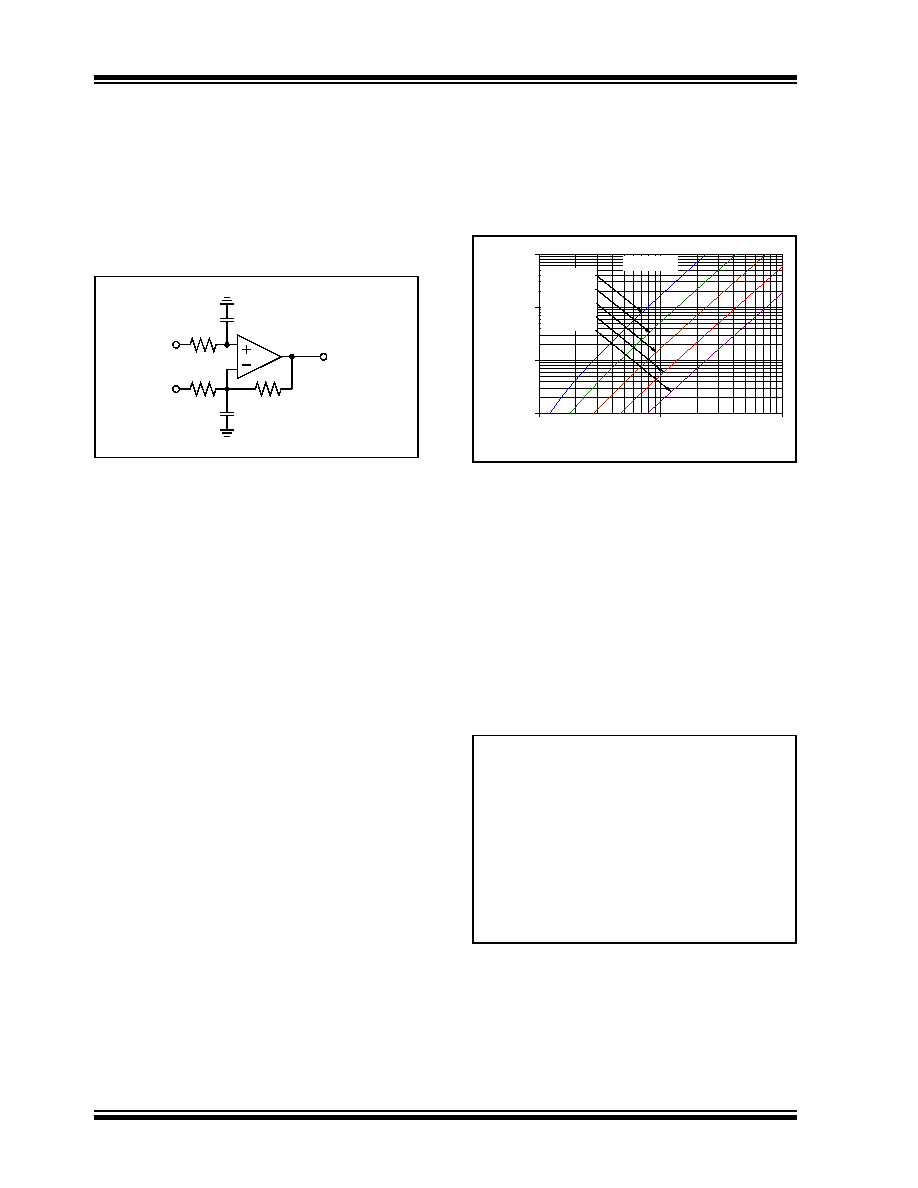
GAIN PEAKING
Figure 4-8 shows an op amp circuit that represents
non-inverting amplifiers (VM is a DC voltage and VP is
the input) or inverting amplifiers (VP is a DC voltage
and VM is the input). The capacitances CN and CG rep-
resent the total capacitance at the input pins; they
include the op amp’s Common mode input capacitance
(CCM), board parasitic capacitance and any capacitor
placed in parallel.
FIGURE 4-8:
Amplifier with Parasitic
Capacitance.
CG acts in parallel with RG (except for a gain of +1 V/V),
which causes an increase in gain at high frequencies.
CG also reduces the phase margin of the feedback
loop, which becomes less stable. This effect can be
reduced by either reducing CG or RF.
CN and RN form a low-pass filter that affects the signal
at VP. This filter has a single real pole at 1/(2RNCN).
The largest value of RF that should be used, depends
several CG values. Some applications may modify
these values to reduce either output loading or gain
peaking (step response overshoot).
FIGURE 4-9:
Maximum Recommended
RF vs. Gain.
Figure 2-35 and Figure 2-36 show the small signal and
large signal step responses at G = +1 V/V. The unity
gain buffer usually has RF = 0 and RG open.
Figure 2-37 and Figure 2-38 show the small signal and
large signal step responses at G = -1 V/V. Since the
noise gain is 2 V/V and CG 10 pF, the resistors were
chosen to be RF = RG = 401 and RN = 200.
It is also possible to add a capacitor (CF) in parallel with
RF to compensate for the destabilizing effect of CG.
This makes it possible to use larger values of RF. The
conditions for stability are summarized in Equation 4-6.
EQUATION 4-6:
VP
RF
VOUT
RN
CN
VM
RG
CG
MCP66X
1.E+02
1.E+03
1.E+04
1.E+05
110
100
Noise Gain; GN (V/V)
M
axi
m
u
m
R
eco
m
en
d
ed
R
F
(
)
GN > +1 V/V
100
10k
100k
1k
CG = 10 pF
CG = 32 pF
CG = 100 pF
CG = 320 pF
CG = 1 nF
fF fGBWP 2GN2
, GN1 GN2
We need:
GN1
1
RF RG
+
=
GN2
1
CG CF
+
=
fF
12
R
FCF
=
fZ
fF GN1 GN2
=
Given:
fF fGBWP 4GN1
, GN1 GN2
相关PDF资料 |
PDF描述 |
|---|---|
| MCP6H04T-E/SL | IC OPAMP QUAD16V 1.2MHZ 14SOIC |
| MCP6N11T-100E/SN | IC AMP INSTR RRIO 35MHZ 8SOIC |
| MCP6V11T-E/OT | IC OPAMP SGL ZERO DRIFT SOT23-5 |
| MCP6V27T-E/SN | IC OPAMP DUAL AUTO-ZERO 8SOIC |
| MCP6V31UT-E/LT | IC OPAMP SGL ZERO DRIFT SC70-5 |
相关代理商/技术参数 |
参数描述 |
|---|---|
| MCP6G01-E/MS | 功能描述:特殊用途放大器 Single Selectable Gain Amplifiers RoHS:否 制造商:Texas Instruments 通道数量:Single 共模抑制比(最小值): 输入补偿电压: 工作电源电压:3 V to 5.5 V 电源电流:5 mA 最大功率耗散: 最大工作温度:+ 70 C 最小工作温度:- 40 C 安装风格:SMD/SMT 封装 / 箱体:QFN-20 封装:Reel |
| MCP6G01-E/P | 制造商:Microchip Technology Inc 功能描述:SINGLE 1.8V, 1 MHZ GAIN BLOCK, E TEMP - Rail/Tube |
| MCP6G01-E/SN | 功能描述:特殊用途放大器 Single Selectable Gain Amplifiers RoHS:否 制造商:Texas Instruments 通道数量:Single 共模抑制比(最小值): 输入补偿电压: 工作电源电压:3 V to 5.5 V 电源电流:5 mA 最大功率耗散: 最大工作温度:+ 70 C 最小工作温度:- 40 C 安装风格:SMD/SMT 封装 / 箱体:QFN-20 封装:Reel |
| MCP6G01RT-E/OT | 功能描述:特殊用途放大器 Sngl 1.8V1MHz Gain Blk E temp RoHS:否 制造商:Texas Instruments 通道数量:Single 共模抑制比(最小值): 输入补偿电压: 工作电源电压:3 V to 5.5 V 电源电流:5 mA 最大功率耗散: 最大工作温度:+ 70 C 最小工作温度:- 40 C 安装风格:SMD/SMT 封装 / 箱体:QFN-20 封装:Reel |
| MCP6G01T-E/MS | 功能描述:特殊用途放大器 Single Selectable Gain Amplifiers RoHS:否 制造商:Texas Instruments 通道数量:Single 共模抑制比(最小值): 输入补偿电压: 工作电源电压:3 V to 5.5 V 电源电流:5 mA 最大功率耗散: 最大工作温度:+ 70 C 最小工作温度:- 40 C 安装风格:SMD/SMT 封装 / 箱体:QFN-20 封装:Reel |
发布紧急采购,3分钟左右您将得到回复。