参数资料
| 型号: | MCP669T-E/ML |
| 厂商: | Microchip Technology |
| 文件页数: | 19/68页 |
| 文件大小: | 0K |
| 描述: | IC OPAMP QUAD 60MHZ 16QFN |
| 标准包装: | 3,300 |
| 放大器类型: | 通用 |
| 电路数: | 4 |
| 输出类型: | 满摆幅 |
| 转换速率: | 32 V/µs |
| 增益带宽积: | 60MHz |
| 电流 - 输入偏压: | 6pA |
| 电压 - 输入偏移: | 1800µV |
| 电流 - 电源: | 6mA |
| 电流 - 输出 / 通道: | 80mA |
| 电压 - 电源,单路/双路(±): | 2.5 V ~ 5.5 V,±1.25 V ~ 2.75 V |
| 工作温度: | -40°C ~ 125°C |
| 安装类型: | 表面贴装 |
| 封装/外壳: | 16-VQFN 裸露焊盘 |
| 供应商设备封装: | 16-QFN(4x4) |
| 包装: | 带卷 (TR) |
第1页第2页第3页第4页第5页第6页第7页第8页第9页第10页第11页第12页第13页第14页第15页第16页第17页第18页当前第19页第20页第21页第22页第23页第24页第25页第26页第27页第28页第29页第30页第31页第32页第33页第34页第35页第36页第37页第38页第39页第40页第41页第42页第43页第44页第45页第46页第47页第48页第49页第50页第51页第52页第53页第54页第55页第56页第57页第58页第59页第60页第61页第62页第63页第64页第65页第66页第67页第68页
MCP660/1/2/3/4/5/9
DS22194D-page 26
2009-2012 Microchip Technology Inc.
4.8
Typical Applications
4.8.1
50
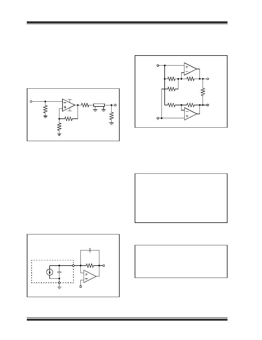
LINE DRIVER
Figure 4-10 shows the MCP661 driving a 50
line. The
large output current (e.g., see Figure 2-18) makes it
possible to drive a back-matched line (RM2, the 50
line and the 50
load at the far end) to more than ±2V
(the load at the far end sees ±1V). It is worth mention-
ing that the 50
line and the 50 load at the far end
together can be modeled as a simple 50
resistor to
ground.
FIGURE 4-10:
50
Line Driver.
The output headroom limits would be VOL = -2.3V and
room for the ±2V signal. The open-loop gain (AOL)
typically does not decrease significantly with a 100
load (see Figure 2-11). The maximum power dissipated
is about 48 mW (see Section 4.2.3 “Power
Dissipation”), so the temperature rise (for the
MCP661 in the SOIC-8 package) is under 8°C.
4.8.2
OPTICAL DETECTOR AMPLIFIER
Figure 4-11 shows a transimpedance amplifier, using
the MCP661 op amp, in a photo detector circuit. The
photo detector is a capacitive current source. RF pro-
vides enough gain to produce 10 mV at VOUT. CF stabi-
lizes the gain and limits the transimpedance bandwidth
to about 1.1 MHz. The parasitic capacitance of RF (e.g.,
0.2 pF for a 0805 SMD) acts in parallel with CF.
FIGURE 4-11:
Transimpedance Amplifier
for an Optical Detector.
4.8.3
H-BRIDGE DRIVER
Figure 4-12 shows the MCP662 dual op amp used as
an H-bridge driver. The load could be a speaker or a
DC motor.
FIGURE 4-12:
H-Bridge Driver.
This circuit automatically makes the noise gains (GN)
equal, when the gains are set properly, so that the fre-
quency responses match well (in magnitude and in
RGB so that both op amps have the same DC gains;
GDM needs to be selected first.
EQUATION 4-7:
Equation 4-8 gives the resulting Common mode and
Differential mode output voltages.
EQUATION 4-8:
RF
301
RG
301
RM1
49.9
50
RM2
49.9
50
Line
+2.5V
-2.5V
MCP66X
Photo
Detector
CD
CF
RF
VDD/2
30pF
100 k
1.5 pF
ID
100 nA
VOUT
MCP661
RF
VIN
VOT
RF
RGB
VOB
VDD/2
RGT
RL
MCP662
GDM
VOT VOB
–
VIN VDD 2
–
--------------------------------- 1 V/V
RGT
RF
GDM 2
1
–
---------------------------------
=
RGB
RF
GDM 2
-------------------
=
VOT V
+ OB
2
---------------------------
VDD
2
-----------
=
VOT V
– OB
GDM VIN
VDD
2
-----------
–
=
相关PDF资料 |
PDF描述 |
|---|---|
| MCP6H04T-E/SL | IC OPAMP QUAD16V 1.2MHZ 14SOIC |
| MCP6N11T-100E/SN | IC AMP INSTR RRIO 35MHZ 8SOIC |
| MCP6V11T-E/OT | IC OPAMP SGL ZERO DRIFT SOT23-5 |
| MCP6V27T-E/SN | IC OPAMP DUAL AUTO-ZERO 8SOIC |
| MCP6V31UT-E/LT | IC OPAMP SGL ZERO DRIFT SC70-5 |
相关代理商/技术参数 |
参数描述 |
|---|---|
| MCP6G01-E/MS | 功能描述:特殊用途放大器 Single Selectable Gain Amplifiers RoHS:否 制造商:Texas Instruments 通道数量:Single 共模抑制比(最小值): 输入补偿电压: 工作电源电压:3 V to 5.5 V 电源电流:5 mA 最大功率耗散: 最大工作温度:+ 70 C 最小工作温度:- 40 C 安装风格:SMD/SMT 封装 / 箱体:QFN-20 封装:Reel |
| MCP6G01-E/P | 制造商:Microchip Technology Inc 功能描述:SINGLE 1.8V, 1 MHZ GAIN BLOCK, E TEMP - Rail/Tube |
| MCP6G01-E/SN | 功能描述:特殊用途放大器 Single Selectable Gain Amplifiers RoHS:否 制造商:Texas Instruments 通道数量:Single 共模抑制比(最小值): 输入补偿电压: 工作电源电压:3 V to 5.5 V 电源电流:5 mA 最大功率耗散: 最大工作温度:+ 70 C 最小工作温度:- 40 C 安装风格:SMD/SMT 封装 / 箱体:QFN-20 封装:Reel |
| MCP6G01RT-E/OT | 功能描述:特殊用途放大器 Sngl 1.8V1MHz Gain Blk E temp RoHS:否 制造商:Texas Instruments 通道数量:Single 共模抑制比(最小值): 输入补偿电压: 工作电源电压:3 V to 5.5 V 电源电流:5 mA 最大功率耗散: 最大工作温度:+ 70 C 最小工作温度:- 40 C 安装风格:SMD/SMT 封装 / 箱体:QFN-20 封装:Reel |
| MCP6G01T-E/MS | 功能描述:特殊用途放大器 Single Selectable Gain Amplifiers RoHS:否 制造商:Texas Instruments 通道数量:Single 共模抑制比(最小值): 输入补偿电压: 工作电源电压:3 V to 5.5 V 电源电流:5 mA 最大功率耗散: 最大工作温度:+ 70 C 最小工作温度:- 40 C 安装风格:SMD/SMT 封装 / 箱体:QFN-20 封装:Reel |
发布紧急采购,3分钟左右您将得到回复。