- 您现在的位置:买卖IC网 > PDF目录98018 > MJE18004D2AF (ON SEMICONDUCTOR) 5 A, 450 V, NPN, Si, POWER TRANSISTOR PDF资料下载
参数资料
| 型号: | MJE18004D2AF |
| 厂商: | ON SEMICONDUCTOR |
| 元件分类: | 功率晶体管 |
| 英文描述: | 5 A, 450 V, NPN, Si, POWER TRANSISTOR |
| 封装: | PLASTIC, TO-220AB, 3 PIN |
| 文件页数: | 18/67页 |
| 文件大小: | 534K |
| 代理商: | MJE18004D2AF |
第1页第2页第3页第4页第5页第6页第7页第8页第9页第10页第11页第12页第13页第14页第15页第16页第17页当前第18页第19页第20页第21页第22页第23页第24页第25页第26页第27页第28页第29页第30页第31页第32页第33页第34页第35页第36页第37页第38页第39页第40页第41页第42页第43页第44页第45页第46页第47页第48页第49页第50页第51页第52页第53页第54页第55页第56页第57页第58页第59页第60页第61页第62页第63页第64页第65页第66页第67页
Surface Mount Package Information and Tape and Reel Specifications
4–2
Motorola Bipolar Power Transistor Device Data
INFORMATION FOR USING SURFACE MOUNT PACKAGES
RECOMMENDED FOOTPRINTS FOR SURFACE MOUNTED APPLICATIONS
Surface mount board layout is a critical portion of the total
design. The footprint for the semiconductor packages must
be the correct size to ensure proper solder connection inter-
face between the board and the package. With the correct
pad geometry, the packages will self align when subjected to
a solder reflow process.
POWER DISSIPATION FOR A SURFACE MOUNT DEVICE
The values for the equation are found in the maximum
ratings table on the data sheet. Substituting these values into
the equation for an ambient temperature TA of 25°C, one can
calculate the power dissipation of the device. For example,
for a D2PAK, PD is calculated as follows.
PD =
150
°C – 25°C
50
°C/W
= 2.5 watts
The 50
°C/W for the D2PAK package assumes the use of
the recommended footprint on a glass epoxy printed circuit
board to achieve a power dissipation of 2.5 watts. There are
other alternatives to achieving higher power dissipation from
the surface mount packages. One is to increase the area of
the drain/collector pad. By increasing the area of the drain/
collector pad, the power dissipation can be increased.
Although the power dissipation can almost be doubled with
this method, area is taken up on the printed circuit board
which can defeat the purpose of using surface mount
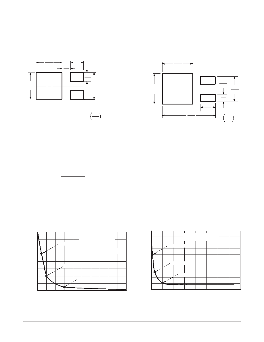
technology. For example, a graph of R
θJA versus drain pad
area is shown in Figures 1 and 2.
Another alternative would be to use a ceramic substrate or
an aluminum core board such as Thermal Clad
. Using a
board material such as Thermal Clad, an aluminum core
board, the power dissipation can be doubled using the same
footprint.
DPAK
0.19
0
4.82
6
mm
inches
0.10
0
2.54
0.063
1.6
0.165
4.191
0.118
3.0
0.243
6.172
D2PAK
mm
inches
0.33
8.38
0.08
2.032
0.04
1.016
0.63
17.02
0.42
10.6
6
0.1
2
3.0
5
0.24
6.096
1.75 Watts
Board Material = 0.0625
″
G–10/FR–4, 2 oz Copper
80
100
60
40
20
10
8
6
4
2
0
3.0 Watts
5.0 Watts
TA = 25°C
A, AREA (SQUARE INCHES)
T
O
AMBIENT
(
C/W)°
R
JA
,T
HERM
AL
RESIS
TA
NCE,
JUNC
T
ION
θ
Figure 1. Thermal Resistance versus Drain Pad
Area for the DPAK Package (Typical)
Figure 2. Thermal Resistance versus Drain Pad
Area for the D2PAK Package (Typical)
2.5 Watts
A, AREA (SQUARE INCHES)
Board Material = 0.0625
″
G–10/FR–4, 2 oz Copper
TA = 25°C
60
70
50
40
30
20
16
14
12
10
8
6
4
2
0
3.5 Watts
5 Watts
T
O
AMBIENT
(
C/W)°
R
JA
,T
HERM
AL
RESIS
TA
NCE,
JUNC
T
ION
θ
相关PDF资料 |
PDF描述 |
|---|---|
| MJE18004D2BA | 5 A, 450 V, NPN, Si, POWER TRANSISTOR |
| MJE18004D2BC | 5 A, 450 V, NPN, Si, POWER TRANSISTOR |
| MJE18004D2AN | 5 A, 450 V, NPN, Si, POWER TRANSISTOR |
| MJE18006AJ | 6 A, 450 V, NPN, Si, POWER TRANSISTOR |
| MJE18006AK | 6 A, 450 V, NPN, Si, POWER TRANSISTOR |
相关代理商/技术参数 |
参数描述 |
|---|---|
| MJE18004D2G | 功能描述:两极晶体管 - BJT 5A 1000V 75W NPN RoHS:否 制造商:STMicroelectronics 配置: 晶体管极性:PNP 集电极—基极电压 VCBO: 集电极—发射极最大电压 VCEO:- 40 V 发射极 - 基极电压 VEBO:- 6 V 集电极—射极饱和电压: 最大直流电集电极电流: 增益带宽产品fT: 直流集电极/Base Gain hfe Min:100 A 最大工作温度: 安装风格:SMD/SMT 封装 / 箱体:PowerFLAT 2 x 2 |
| MJE18004G | 功能描述:两极晶体管 - BJT 5A 1000V 75W NPN RoHS:否 制造商:STMicroelectronics 配置: 晶体管极性:PNP 集电极—基极电压 VCBO: 集电极—发射极最大电压 VCEO:- 40 V 发射极 - 基极电压 VEBO:- 6 V 集电极—射极饱和电压: 最大直流电集电极电流: 增益带宽产品fT: 直流集电极/Base Gain hfe Min:100 A 最大工作温度: 安装风格:SMD/SMT 封装 / 箱体:PowerFLAT 2 x 2 |
| MJE18006 | 功能描述:两极晶体管 - BJT 6A 450V 100W NPN RoHS:否 制造商:STMicroelectronics 配置: 晶体管极性:PNP 集电极—基极电压 VCBO: 集电极—发射极最大电压 VCEO:- 40 V 发射极 - 基极电压 VEBO:- 6 V 集电极—射极饱和电压: 最大直流电集电极电流: 增益带宽产品fT: 直流集电极/Base Gain hfe Min:100 A 最大工作温度: 安装风格:SMD/SMT 封装 / 箱体:PowerFLAT 2 x 2 |
| MJE18006G | 功能描述:两极晶体管 - BJT BIP NPN 8A 450V RoHS:否 制造商:STMicroelectronics 配置: 晶体管极性:PNP 集电极—基极电压 VCBO: 集电极—发射极最大电压 VCEO:- 40 V 发射极 - 基极电压 VEBO:- 6 V 集电极—射极饱和电压: 最大直流电集电极电流: 增益带宽产品fT: 直流集电极/Base Gain hfe Min:100 A 最大工作温度: 安装风格:SMD/SMT 封装 / 箱体:PowerFLAT 2 x 2 |
| MJE18008 | 功能描述:两极晶体管 - BJT 8A 450V 125W NPN RoHS:否 制造商:STMicroelectronics 配置: 晶体管极性:PNP 集电极—基极电压 VCBO: 集电极—发射极最大电压 VCEO:- 40 V 发射极 - 基极电压 VEBO:- 6 V 集电极—射极饱和电压: 最大直流电集电极电流: 增益带宽产品fT: 直流集电极/Base Gain hfe Min:100 A 最大工作温度: 安装风格:SMD/SMT 封装 / 箱体:PowerFLAT 2 x 2 |
发布紧急采购,3分钟左右您将得到回复。