- 您现在的位置:买卖IC网 > Datasheet目录344 > MSC8144ADS (Freescale Semiconductor)ADS FOR MSC8144 DEVICE Datasheet资料下载
参数资料
| 型号: | MSC8144ADS |
| 厂商: | Freescale Semiconductor |
| 文件页数: | 35/80页 |
| 文件大小: | 0K |
| 描述: | ADS FOR MSC8144 DEVICE |
| 标准包装: | 1 |
| 类型: | DSP |
| 适用于相关产品: | MSC8144 |
| 所含物品: | AMC 卡、电源、缆线、USB TAP、硬件和说明文档 |
第1页第2页第3页第4页第5页第6页第7页第8页第9页第10页第11页第12页第13页第14页第15页第16页第17页第18页第19页第20页第21页第22页第23页第24页第25页第26页第27页第28页第29页第30页第31页第32页第33页第34页当前第35页第36页第37页第38页第39页第40页第41页第42页第43页第44页第45页第46页第47页第48页第49页第50页第51页第52页第53页第54页第55页第56页第57页第58页第59页第60页第61页第62页第63页第64页第65页第66页第67页第68页第69页第70页第71页第72页第73页第74页第75页第76页第77页第78页第79页第80页
�� �
�
�Electrical� Characteristics�
�2.6�
��The� following� sections� include� illustrations� and� tables� of� clock� diagrams,� signals,� and� parallel� I/O� outputs� and� inputs.�
�2.6.1�
�Start-Up� Timing�
�Starting� the� device� requires� coordination� among� several� input� sequences� including� clocking,� reset,� and� power.� Section� 2.6.2�
�describes� the� clocking� characteristics.� Section� 2.6.3� describes� the� reset� and� power-up� characteristics.� You� must� use� the�
�following� guidelines� when� starting� up� an� MSC8144� device:�
�?�
�Note:�
�?�
�?�
�PORESET� and� TRST� must� be� asserted� externally� for� the� duration� of� the� power-up� sequence� using� the� V� DDIO� (3.3� V)�
�supply.� See� Table� 19� for� timing.� TRST� deassertion� does� not� have� to� be� synchronized� with� PORESET� deassertion.�
�During� functional� operation� when� JTAG� is� not� used,� TRST� can� be� asserted� and� remain� asserted� after� the� power� ramp.�
�For� applications� that� use� M3� memory,� M3_RESET� should� replicate� the� PORESET� sequence� timing,� but� using� the�
�V� DDM3IO� (2.5� V)� supply.� See� Section� 3.1.1� ,� Power-on� Sequence� for� additional� design� information.�
�CLKIN� should� start� toggling� at� least� 32� cycles� before� the� PORESET� deassertion� to� guarantee� correct� device� operation�
�(see� Figure� 6� ).� 32� cycles� should� be� accounted� only� after� V� DDIO� reaches� its� nominal� value.�
�CLKIN� and� PCI_CLK_IN� should� either� be� stable� low� during� the� power-up� of� V� DDIO� supply� and� start� their� swings� after�
�power-up� or� should� swing� within� V� DDIO� range� during� V� DDIO� power-up.,� so� their� amplitude� grows� as� V� DDIO� grows�
�during� power-up.�
�Figure� 6� shows� a� sequence� in� which� V� DDIO� is� raised� after� V� DD� and� CLKIN� begins� to� toggle� with� the� raise� of� V� DDIO� supply.�
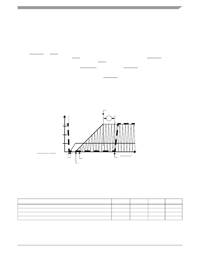
�V� DDIO� =� Nominal�
�V� DD� =� Nominal�
�1�
�3.3� V�
�1.0� V�
�V� DDIO� Nominal�
�V� DD� Nominal�
�Time�
�PORESET/TRST� asserted�
�V� DD� applied�
�CLKIN� starts� toggling�
�PORESET�
�V� DDIO� applied�
�Figure� 6.� Start-Up� Sequence� with� V� DD� Raised� Before� V� DDIO� with� CLKIN� Started� with� V� DDIO�
�2.6.2�
�Clock� and� Timing� Signals�
�The� following� sections� include� a� description� of� clock� signal� characteristics.� Table� 16� shows� the� maximum� frequency� values� for�
�CLKIN� and� PCI_CLK_IN.� The� user� must� ensure� that� maximum� frequency� values� are� not� exceeded.�
�Table� 16.� Clock� Frequencies�
�CLKIN� frequency�
�PCI_CLK_IN� frequency�
�CLKIN� duty� cycle�
�PCI_CLK_IN� duty� cycle�
�Characteristic�
�Symbol�
�F� CLKIN�
�F� PCI_CLK_IN�
�D� CLKIN�
�D� PCI_CLK_IN�
�Min�
�33�
�33�
�40�
�40�
�Max�
�133�
�133�
�60�
�60�
�Unit�
�MHz�
�MHz�
�%�
�%�
�MSC8144� Quad� Core� Digital� Signal� Processor� Data� Sheet,� Rev.� 16�
�Freescale� Semiconductor�
�35�
�相关PDF资料 |
PDF描述 |
|---|---|
| MSC8156EVM | EVAL MODULE FOR MSC8156 LC |
| MSL1060AW | IC LED DRIVER 6 STRING |
| MSL1061AV | IC LED DRIVER 6 STRING |
| MSL2041GU | IC LED DRIVER 4 STRING |
| MSL2100BR | IC LED DRIVER 8 STRING |
相关代理商/技术参数 |
参数描述 |
|---|---|
| MSC8144AMC-SA | 制造商:Freescale Semiconductor 功能描述:BOARD AMC SGL WIDTH MSC8144 DSP |
| MSC8144E | 制造商:FREESCALE 制造商全称:Freescale Semiconductor, Inc 功能描述:Quad Core Digital Signal Processor |
| MSC8144EC | 制造商:FREESCALE 制造商全称:Freescale Semiconductor, Inc 功能描述:Quad Core Digital Signal Processor |
| MSC8144ESVT1000B | 制造商:Freescale Semiconductor 功能描述:DSP 32-BIT 1GHZ 1000MIPS 783-PIN FCBGA BOX - Trays 制造商:Freescale Semiconductor 功能描述:ENCRYPTION PACSUN R2.1 783FCPBGA |
| MSC8144ESVT800A | 制造商:Freescale Semiconductor 功能描述:DSP 32BIT 800MHZ 800MIPS 783FCBGA - Trays |
发布紧急采购,3分钟左右您将得到回复。