- 您现在的位置:买卖IC网 > PDF目录189002 > NAND256W3A2CZA1E (NUMONYX) 32M X 8 FLASH 3V PROM, 35 ns, PBGA55 PDF资料下载
参数资料
| 型号: | NAND256W3A2CZA1E |
| 厂商: | NUMONYX |
| 元件分类: | PROM |
| 英文描述: | 32M X 8 FLASH 3V PROM, 35 ns, PBGA55 |
| 封装: | 8 X 10 MM, 1 MM HEIGHT, 0.80 MM PITCH, ROHS COMPLIANT, VFBGA-55 |
| 文件页数: | 18/57页 |
| 文件大小: | 916K |
| 代理商: | NAND256W3A2CZA1E |
第1页第2页第3页第4页第5页第6页第7页第8页第9页第10页第11页第12页第13页第14页第15页第16页第17页当前第18页第19页第20页第21页第22页第23页第24页第25页第26页第27页第28页第29页第30页第31页第32页第33页第34页第35页第36页第37页第38页第39页第40页第41页第42页第43页第44页第45页第46页第47页第48页第49页第50页第51页第52页第53页第54页第55页第56页第57页
25/57
NAND128-A, NAND256-A, NAND512-A, NAND01G-A
Page Program
The Page Program operation is the standard oper-
ation to program data to the memory array.
The main area of the memory array is pro-
grammed by page, however partial page program-
ming is allowed where any number of bytes (1 to
528) or words (1 to 264) can be programmed.
The maximum number of consecutive partial page
program operations allowed in the same page is
three. After exceeding this a Block Erase com-
mand must be issued before any further program
operations can take place in that page.
Before starting a Page Program operation a Point-
er operation can be performed to point to the area
to be programmed. Refer to the Pointer Opera-
tions section and Figure 12. for details.
Each Page Program operation consists of five
steps (see Figure 17.):
1.
one bus cycle is required to setup the Page
Program command
2.
four bus cycles are then required to input the
program address (refer to Table 6.)
3.
the data is then input (up to 528 Bytes/ 264
Words) and loaded into the Page Buffer
4.
one bus cycle is required to issue the confirm
command to start the P/E/R Controller.
5.
The P/E/R Controller then programs the data
into the array.
Once the program operation has started the Sta-
tus Register can be read using the Read Status
Register command. During program operations
the Status Register will only flag errors for bits set
to '1' that have not been successfully programmed
to '0'.
During the program operation, only the Read Sta-
tus Register and Reset commands will be accept-
ed, all other commands will be ignored.
Once the program operation has completed the P/
E/R Controller bit SR6 is set to ‘1’ and the Ready/
Busy signal goes High.
The device remains in Read Status Register mode
until another valid command is written to the Com-
mand Interface.
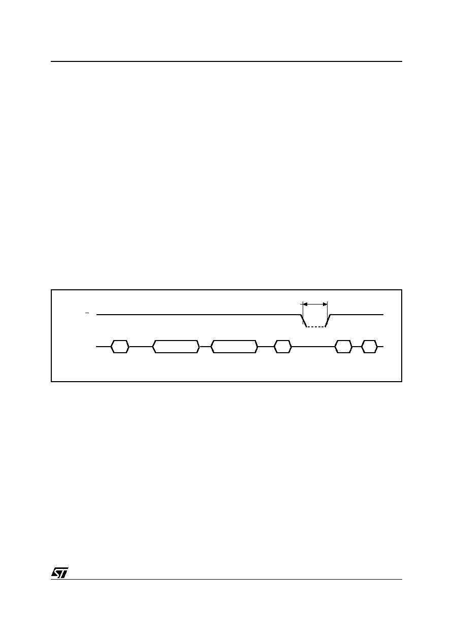
Figure 17. Page Program Operation
Note: Before starting a Page Program operation a Pointer operation can be performed. Refer to Pointer Operations section for details.
I/O
RB
Address Inputs
SR0
ai07566
Data Input
10h
70h
80h
Page Program
Setup Code
Confirm
Code
Read Status Register
Busy
tBLBH2
(Program Busy time)
相关PDF资料 |
PDF描述 |
|---|---|
| NAND01GR4A2AZB6 | 64M X 16 FLASH 1.8V PROM, 35 ns, PBGA63 |
| NAND01GW3B2CN1E | 128M X 8 FLASH 3V PROM, 25000 ns, PDSO48 |
| NAND04GR3B3AN6 | 512M X 8 FLASH 1.8V PROM, 35 ns, PDSO48 |
| NAND512W3B3BZA1F | 64M X 8 FLASH 3V PROM, 35 ns, PBGA63 |
| NAND512W3B3CV1 | 64M X 8 FLASH 3V PROM, 35 ns, PDSO48 |
相关代理商/技术参数 |
参数描述 |
|---|---|
| NAND256W4A0AN6E | 功能描述:闪存 NAND & S.MEDIA FLASH RoHS:否 制造商:ON Semiconductor 数据总线宽度:1 bit 存储类型:Flash 存储容量:2 MB 结构:256 K x 8 定时类型: 接口类型:SPI 访问时间: 电源电压-最大:3.6 V 电源电压-最小:2.3 V 最大工作电流:15 mA 工作温度:- 40 C to + 85 C 安装风格:SMD/SMT 封装 / 箱体: 封装:Reel |
| NAND32GAH0HZA5E | 制造商:Micron Technology Inc 功能描述:NAND EMMC - Trays |
| NAND32GAH0HZA5F | 制造商:Micron Technology Inc 功能描述:NAND EMMC - Tape and Reel |
| NAND32GAH0PZA5E | 制造商:Micron Technology Inc 功能描述:EMMC 4.3 4GB 12X16 41NM - Trays |
| NAND32GAH0PZA5F | 制造商:Micron Technology Inc 功能描述:NAND EMMC - Tape and Reel |
发布紧急采购,3分钟左右您将得到回复。