- 您现在的位置:买卖IC网 > PDF目录189002 > NAND256W3A2CZA1E (NUMONYX) 32M X 8 FLASH 3V PROM, 35 ns, PBGA55 PDF资料下载
参数资料
| 型号: | NAND256W3A2CZA1E |
| 厂商: | NUMONYX |
| 元件分类: | PROM |
| 英文描述: | 32M X 8 FLASH 3V PROM, 35 ns, PBGA55 |
| 封装: | 8 X 10 MM, 1 MM HEIGHT, 0.80 MM PITCH, ROHS COMPLIANT, VFBGA-55 |
| 文件页数: | 24/57页 |
| 文件大小: | 916K |
| 代理商: | NAND256W3A2CZA1E |
第1页第2页第3页第4页第5页第6页第7页第8页第9页第10页第11页第12页第13页第14页第15页第16页第17页第18页第19页第20页第21页第22页第23页当前第24页第25页第26页第27页第28页第29页第30页第31页第32页第33页第34页第35页第36页第37页第38页第39页第40页第41页第42页第43页第44页第45页第46页第47页第48页第49页第50页第51页第52页第53页第54页第55页第56页第57页
NAND128-A, NAND256-A, NAND512-A, NAND01G-A
30/57
SOFTWARE ALGORITHMS
This section gives information on the software al-
gorithms that ST recommends to implement to
manage the Bad Blocks and extend the lifetime of
the NAND device.
NAND Flash memories are programmed and
erased by Fowler-Nordheim tunneling using a high
voltage. Exposing the device to a high voltage for
extended periods can cause the oxide layer to be
damaged. For this reason, the number of program
and erase cycles is limited (see Table 14. for val-
ue) and it is recommended to implement Garbage
Collection, a Wear-Leveling Algorithm and an Er-
ror Correction Code, to extend the number of pro-
gram and erase cycles and increase the data
retention.
To help integrate a NAND memory into an applica-
tion ST Microelectronics can provide:
■
File System OS Native reference software,
which supports the basic commands of file
management.
Contact the nearest ST Microelectronics sales of-
fice for more details.
Bad Block Management
Devices with Bad Blocks have the same quality
level and the same AC and DC characteristics as
devices where all the blocks are valid. A Bad Block
does not affect the performance of valid blocks be-
cause it is isolated from the bit line and common
source line by a select transistor.
The devices are supplied with all the locations in-
side valid blocks erased (FFh). The Bad Block In-
formation is written prior to shipping. Any block
where the 6th Byte/ 1st Word in the spare area of
the 1st page does not contain FFh is a Bad Block.
The Bad Block Information must be read before
any erase is attempted as the Bad Block Informa-
tion may be erased. For the system to be able to
recognize the Bad Blocks based on the original in-
formation it is recommended to create a Bad Block
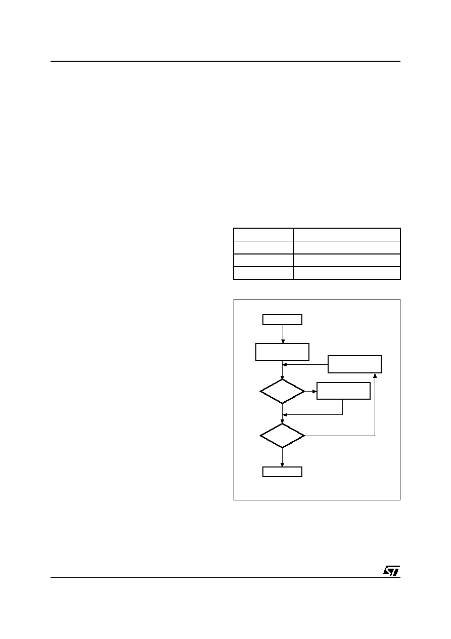
table following the flowchart shown in Figure 20.
Block Replacement
Over the lifetime of the device additional Bad
Blocks may develop. In this case the block has to
be replaced by copying the data to a valid block.
These additional Bad Blocks can be identified as
attempts to program or erase them will give errors
in the Status Register.
As the failure of a page program operation does
not affect the data in other pages in the same
block, the block can be replaced by re-program-
ming the current data and copying the rest of the
replaced block to an available valid block. The
Copy Back Program command can be used to
copy the data to a valid block.
See the “Copy Back Program” section for more de-
tails.
Refer to Table 13. for the recommended proce-
dure to follow if an error occurs during an opera-
tion.
Table 13. Block Failure
Figure 20. Bad Block Management Flowchart
Operation
Recommended Procedure
Erase
Block Replacement
Program
Block Replacement or ECC
Read
ECC
AI07588C
START
END
NO
YES
NO
Block Address =
Block 0
Data
= FFh?
Last
block?
Increment
Block Address
Update
Bad Block table
相关PDF资料 |
PDF描述 |
|---|---|
| NAND01GR4A2AZB6 | 64M X 16 FLASH 1.8V PROM, 35 ns, PBGA63 |
| NAND01GW3B2CN1E | 128M X 8 FLASH 3V PROM, 25000 ns, PDSO48 |
| NAND04GR3B3AN6 | 512M X 8 FLASH 1.8V PROM, 35 ns, PDSO48 |
| NAND512W3B3BZA1F | 64M X 8 FLASH 3V PROM, 35 ns, PBGA63 |
| NAND512W3B3CV1 | 64M X 8 FLASH 3V PROM, 35 ns, PDSO48 |
相关代理商/技术参数 |
参数描述 |
|---|---|
| NAND256W4A0AN6E | 功能描述:闪存 NAND & S.MEDIA FLASH RoHS:否 制造商:ON Semiconductor 数据总线宽度:1 bit 存储类型:Flash 存储容量:2 MB 结构:256 K x 8 定时类型: 接口类型:SPI 访问时间: 电源电压-最大:3.6 V 电源电压-最小:2.3 V 最大工作电流:15 mA 工作温度:- 40 C to + 85 C 安装风格:SMD/SMT 封装 / 箱体: 封装:Reel |
| NAND32GAH0HZA5E | 制造商:Micron Technology Inc 功能描述:NAND EMMC - Trays |
| NAND32GAH0HZA5F | 制造商:Micron Technology Inc 功能描述:NAND EMMC - Tape and Reel |
| NAND32GAH0PZA5E | 制造商:Micron Technology Inc 功能描述:EMMC 4.3 4GB 12X16 41NM - Trays |
| NAND32GAH0PZA5F | 制造商:Micron Technology Inc 功能描述:NAND EMMC - Tape and Reel |
发布紧急采购,3分钟左右您将得到回复。