- 您现在的位置:买卖IC网 > PDF目录189449 > OR4E063BA352-DB (LATTICE SEMICONDUCTOR CORP) FPGA, 2024 CLBS, 515000 GATES, PBGA352 PDF资料下载
参数资料
| 型号: | OR4E063BA352-DB |
| 厂商: | LATTICE SEMICONDUCTOR CORP |
| 元件分类: | FPGA |
| 英文描述: | FPGA, 2024 CLBS, 515000 GATES, PBGA352 |
| 封装: | PLASTIC, BGA-352 |
| 文件页数: | 124/151页 |
| 文件大小: | 2680K |
| 代理商: | OR4E063BA352-DB |
第1页第2页第3页第4页第5页第6页第7页第8页第9页第10页第11页第12页第13页第14页第15页第16页第17页第18页第19页第20页第21页第22页第23页第24页第25页第26页第27页第28页第29页第30页第31页第32页第33页第34页第35页第36页第37页第38页第39页第40页第41页第42页第43页第44页第45页第46页第47页第48页第49页第50页第51页第52页第53页第54页第55页第56页第57页第58页第59页第60页第61页第62页第63页第64页第65页第66页第67页第68页第69页第70页第71页第72页第73页第74页第75页第76页第77页第78页第79页第80页第81页第82页第83页第84页第85页第86页第87页第88页第89页第90页第91页第92页第93页第94页第95页第96页第97页第98页第99页第100页第101页第102页第103页第104页第105页第106页第107页第108页第109页第110页第111页第112页第113页第114页第115页第116页第117页第118页第119页第120页第121页第122页第123页当前第124页第125页第126页第127页第128页第129页第130页第131页第132页第133页第134页第135页第136页第137页第138页第139页第140页第141页第142页第143页第144页第145页第146页第147页第148页第149页第150页第151页
74
Lattice Semiconductor
Data Sheet
September, 2002
ORCA Series 4 FPGAs
FPGA Conguration Modes (continued)
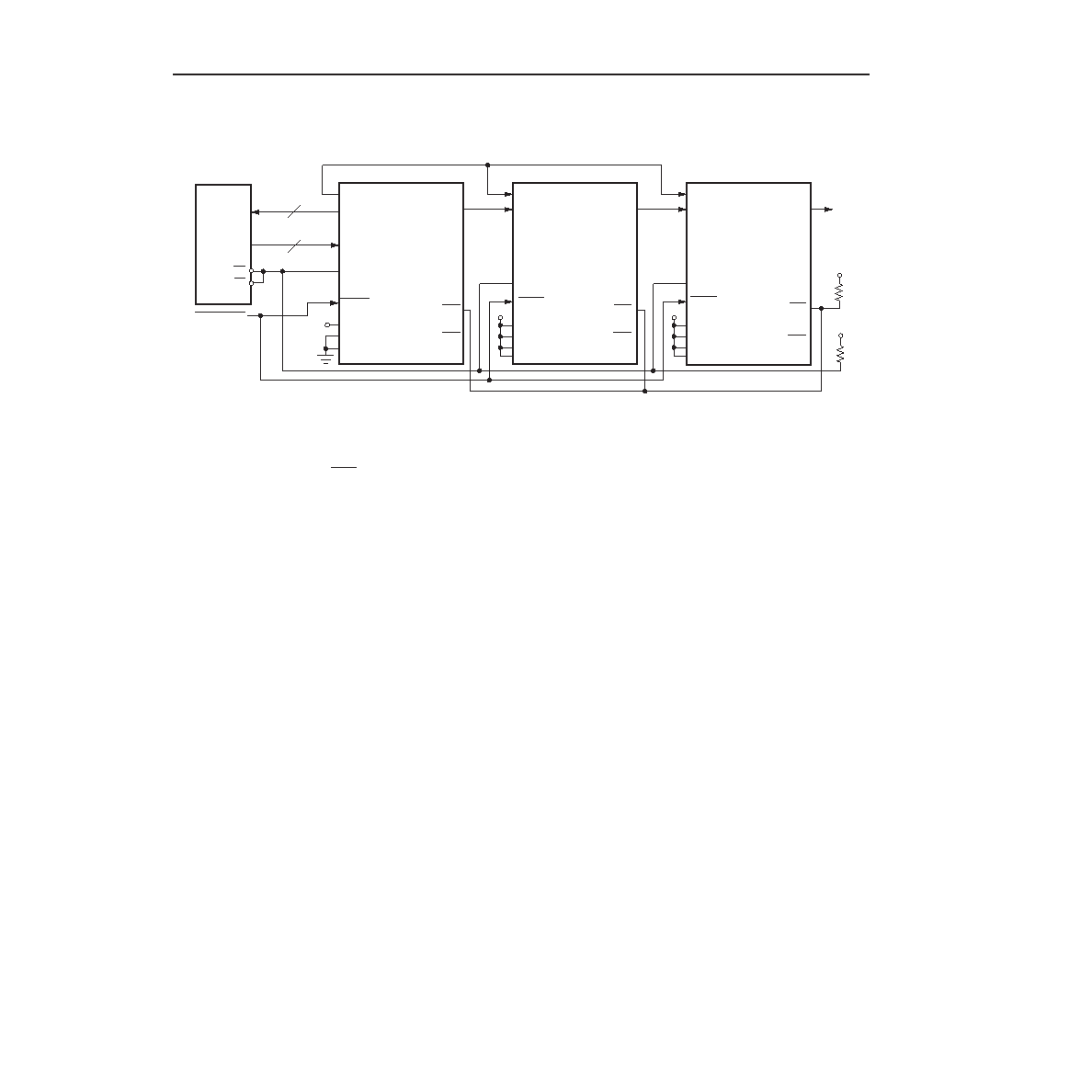
5-4488(F).a
Figure 46. Daisy-Chain Conguration Schematic
As seen in Figure 46, the INIT pins for all of the FPGAs are connected together. This is required to guarantee that
powerup and initialization will work correctly. In general, the DONE pins for all of the FPGAs are also connected
together as shown to guarantee that all of the FPGAs enter the start-up state simultaneously. This may not be
required, depending upon the start-up sequence desired.
Daisy-Chaining with Boundary-Scan
Multiple FPGAs can be congured through the JTAG ports by using a daisy-chain of the FPGAs. This daisy-chain-
ing operation is available upon initial conguration after powerup, after a power-on reset, after pulling the program
pin to reset the chip, or during a reconguration if the EN_JTAG RAM has been set.
All daisy-chained FPGAs are connected in series. Each FPGA reads and shifts the preamble and length count in
on the positive TCK and out on the negative TCK edges.
An upstream FPGA that has received the preamble and length count outputs a high on TDO until it has received
the appropriate number of data frames so that downstream FPGAs do not receive frame start bit pairs. After load-
ing and retransmitting the preamble and length count to a daisy-chain of downstream devices, the lead device
loads its conguration data frames.
The loading of conguration data continues after the lead device had received its conguration read into TDI of
downstream devices on the positive edge of TCK, and shifted out TDO on the negative edge of TCK.
VDD
EPROM
PROGRAM
OE
CE
M2
M1
M0
DONE
HDC
LDC
RCLK
CCLK
DOUT
DIN
DOUT
DIN
CCLK
DONE
DOUT
INIT
CCLK
VDD
PRGM
HDC
LDC
RCLK
HDC
LDC
RCLK
VDD
ORCA
SERIES
FPGA
SLAVE 2
ORCA
SERIES
FPGA
MASTER
ORCA
SERIES
FPGA
SLAVE 1
A[21:0]
D[7:0]
DONE
M3
M2
M1
M0
VDD
M3
M2
M1
M0
VDD
相关PDF资料 |
PDF描述 |
|---|---|
| OR4E063BM680-DB | FPGA, 2024 CLBS, 515000 GATES, PBGA680 |
| ORT4622-8BC432I | FPGA, PBGA432 |
| ORT4622-8BM680I | FPGA, PBGA680 |
| ORT4622-8BC432I | FPGA, PBGA432 |
| ORT4622-8BM680I | FPGA, PBGA680 |
相关代理商/技术参数 |
参数描述 |
|---|---|
| OR4E10 | 制造商:AGERE 制造商全称:AGERE 功能描述:Field-Programmable Gate Arrays |
| OR4E14 | 制造商:未知厂家 制造商全称:未知厂家 功能描述:Field-Programmable Gate Arrays |
| OR4E2 | 制造商:AGERE 制造商全称:AGERE 功能描述:Field-Programmable Gate Arrays |
| OR4E2-1BA256 | 制造商:未知厂家 制造商全称:未知厂家 功能描述:FPGA |
| OR4E2-1BA352 | 制造商:未知厂家 制造商全称:未知厂家 功能描述:FPGA |
发布紧急采购,3分钟左右您将得到回复。