- 您现在的位置:买卖IC网 > PDF目录189449 > OR4E063BA352-DB (LATTICE SEMICONDUCTOR CORP) FPGA, 2024 CLBS, 515000 GATES, PBGA352 PDF资料下载
参数资料
| 型号: | OR4E063BA352-DB |
| 厂商: | LATTICE SEMICONDUCTOR CORP |
| 元件分类: | FPGA |
| 英文描述: | FPGA, 2024 CLBS, 515000 GATES, PBGA352 |
| 封装: | PLASTIC, BGA-352 |
| 文件页数: | 66/151页 |
| 文件大小: | 2680K |
| 代理商: | OR4E063BA352-DB |
第1页第2页第3页第4页第5页第6页第7页第8页第9页第10页第11页第12页第13页第14页第15页第16页第17页第18页第19页第20页第21页第22页第23页第24页第25页第26页第27页第28页第29页第30页第31页第32页第33页第34页第35页第36页第37页第38页第39页第40页第41页第42页第43页第44页第45页第46页第47页第48页第49页第50页第51页第52页第53页第54页第55页第56页第57页第58页第59页第60页第61页第62页第63页第64页第65页当前第66页第67页第68页第69页第70页第71页第72页第73页第74页第75页第76页第77页第78页第79页第80页第81页第82页第83页第84页第85页第86页第87页第88页第89页第90页第91页第92页第93页第94页第95页第96页第97页第98页第99页第100页第101页第102页第103页第104页第105页第106页第107页第108页第109页第110页第111页第112页第113页第114页第115页第116页第117页第118页第119页第120页第121页第122页第123页第124页第125页第126页第127页第128页第129页第130页第131页第132页第133页第134页第135页第136页第137页第138页第139页第140页第141页第142页第143页第144页第145页第146页第147页第148页第149页第150页第151页
Lattice Semiconductor
21
Data Sheet
September, 2002
ORCA Series 4 FPGAs
Programmable Logic Cells (continued)
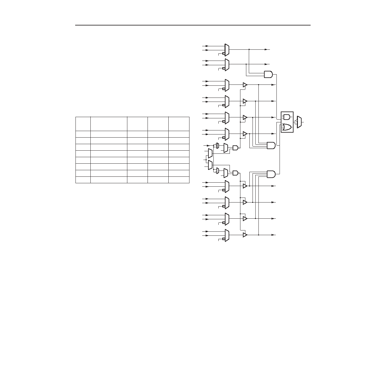
As discussed in the memory mode section, if the SLIC
is placed into one of the modes where it contains both
buffers and a decode or AOI function (e.g.,
BUF_BUF_DEC mode), the DEC output can be gated
with the 3-state input signal. This allows up to a 6-input
decode (e.g., BUF_DEC_DEC mode) plus the 3-state
input to control the enable/disable of up to four buffers
per SLIC Figure 15—Figure 19 show several congura-
tions of the SLIC, while Table 5 shows all of the possi-
ble modes.
Table 5. SLIC Modes
5-5744(F).a.
Figure 14. SLIC All Modes Diagram
Mode
No.
Mode
BUF
[3:0]
BUF
[7:4]
BUF
[9:8]
1BUFFER
Buffer
2BUF_BUF_DEC
Buffer
Decoder
3BUF_DEC_BUF
Buffer
Decoder
Buffer
4
BUF_DEC_DEC
Buffer
Decoder Decoder
5
DEC_BUF_BUF Decoder
Buffer
6
DEC_BUF_DEC
Decoder
Buffer
Decoder
7
DEC_DEC_BUF
Decoder Decoder
Buffer
8
DECODER
Decoder Decoder Decoder
SIN9
I9
SOUT09
DEC
0/1
TRI
0/1
SOUT08
SOUT07
SOUT06
SOUT05
SOUT04
SOUT03
SOUT02
SOUT01
SOUT00
LOGIC 1 OR 0
SIN8
I8
LOGIC 1 OR 0
SIN7
I7
LOGIC 1 OR 0
SIN6
I6
LOGIC 1 OR 0
SIN5
I5
LOGIC 1 OR 0
SIN4
I4
LOGIC 1 OR 0
SIN3
I3
LOGIC 1 OR 0
SIN2
I2
LOGIC 1 OR 0
SIN1
I1
LOGIC 1 OR 0
SIN0
I0
LOGIC 1 OR 0
相关PDF资料 |
PDF描述 |
|---|---|
| OR4E063BM680-DB | FPGA, 2024 CLBS, 515000 GATES, PBGA680 |
| ORT4622-8BC432I | FPGA, PBGA432 |
| ORT4622-8BM680I | FPGA, PBGA680 |
| ORT4622-8BC432I | FPGA, PBGA432 |
| ORT4622-8BM680I | FPGA, PBGA680 |
相关代理商/技术参数 |
参数描述 |
|---|---|
| OR4E10 | 制造商:AGERE 制造商全称:AGERE 功能描述:Field-Programmable Gate Arrays |
| OR4E14 | 制造商:未知厂家 制造商全称:未知厂家 功能描述:Field-Programmable Gate Arrays |
| OR4E2 | 制造商:AGERE 制造商全称:AGERE 功能描述:Field-Programmable Gate Arrays |
| OR4E2-1BA256 | 制造商:未知厂家 制造商全称:未知厂家 功能描述:FPGA |
| OR4E2-1BA352 | 制造商:未知厂家 制造商全称:未知厂家 功能描述:FPGA |
发布紧急采购,3分钟左右您将得到回复。