- 您现在的位置:买卖IC网 > PDF目录367934 > PH28F640L18T85 (INTEL CORP) StrataFlash Wireless Memory PDF资料下载
参数资料
| 型号: | PH28F640L18T85 |
| 厂商: | INTEL CORP |
| 元件分类: | PROM |
| 英文描述: | StrataFlash Wireless Memory |
| 中文描述: | 4M X 16 FLASH 1.8V PROM, 85 ns, PBGA56 |
| 封装: | 0.75 MM PITCH, LEAD FREE, VFBGA-56 |
| 文件页数: | 48/106页 |
| 文件大小: | 1272K |
| 代理商: | PH28F640L18T85 |
第1页第2页第3页第4页第5页第6页第7页第8页第9页第10页第11页第12页第13页第14页第15页第16页第17页第18页第19页第20页第21页第22页第23页第24页第25页第26页第27页第28页第29页第30页第31页第32页第33页第34页第35页第36页第37页第38页第39页第40页第41页第42页第43页第44页第45页第46页第47页当前第48页第49页第50页第51页第52页第53页第54页第55页第56页第57页第58页第59页第60页第61页第62页第63页第64页第65页第66页第67页第68页第69页第70页第71页第72页第73页第74页第75页第76页第77页第78页第79页第80页第81页第82页第83页第84页第85页第86页第87页第88页第89页第90页第91页第92页第93页第94页第95页第96页第97页第98页第99页第100页第101页第102页第103页第104页第105页第106页
Intel StrataFlash Wireless Memory (L18)
April 2005
48
Intel StrataFlash Wireless Memory (L18)
Order Number: 251902, Revision: 009
Datasheet
9.3
Command Definitions
Valid device command codes and descriptions are shown in
Table 9
.
Protection
Program Protection Register
2
Write
PRA
0xC0
Write
PRA
PD
Program Lock Register
2
Write
LRA
0xC0
Write
LRA
LRD
Configuration
Program Read Configuration Register
2
Write
RCD
0x60
Write
RCD
0x03
Notes:
1.
First command cycle address should be the same as the operation’s target address.
PnA = Address within the partition.
PBA = Partition base address.
IA = Identification code address offset.
QA = CFI Query address offset.
BA = Address within the block.
WA = Word address of memory location to be written.
PRA = Protection Register address.
LRA = Lock Register address.
X = Any valid address within the device.
ID = Identifier data.
QD = Query data on DQ[15:0].
SRD = Status Register data.
WD = Word data.
N = Word count of data to be loaded into the write buffer.
PD = Protection Register data.
PD = Protection Register data.
LRD = Lock Register data.
RCD = Read Configuration Register data on A[15:0]. A[MAX:16] can select any partition
.
The second cycle of the Buffered Program Command is the word count of the data to be loaded into the write buffer. This
is followed by up to 32 words of data.Then the confirm command (0xD0) is issued, triggering the array programming
operation.
The confirm command (0xD0) is followed by the buffer data.
2.
3.
4.
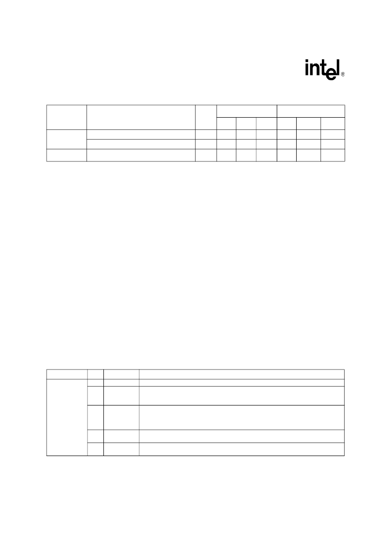
Table 8.
Command Bus Cycles (Sheet 2 of 2)
Mode
Command
Bus
Cycles
First Bus Cycle
Second Bus Cycle
Oper
Addr
1
Data
2
Oper
Addr
1
Data
2
Table 9.
Command Codes and Definitions (Sheet 1 of 2)
Mode
Code Device Mode
0xFF Read Array
Description
Read
Places the addressed partition in Read Array mode. Array data is output on DQ[15:0].
Places the addressed partition in Read Status Register mode. The partition enters this
mode after a program or erase command is issued. Status Register data is output on
DQ[7:0].
0x70Register
0x90
Read Device
ID or
Configuration
Register
Places the addressed partition in Read Device Identifier mode. Subsequent reads from
addresses within the partition outputs manufacturer/device codes, Configuration Register
data, Block Lock status, or Protection Register data on DQ[15:0].
0x98 Read Query
Places the addressed partition in Read Query mode. Subsequent reads from the partition
addresses output Common Flash Interface information on DQ[7:0].
The WSM can only set Status Register error bits. The Clear Status Register command is
used to clear the SR error bits.
0x50Register
相关PDF资料 |
PDF描述 |
|---|---|
| PH2907A | PNP switching transistor |
| PH2907 | PNP switching transistor |
| PH2931-135S | Rail-to-Rail, Very Low Noise Universal Dual Filter Building Block; Package: SO; No of Pins: 16; Temperature Range: -40°C to +85°C |
| PH2931-I3 | Radar Pulsed Power Transistor, 135W, 20ms Pulse, 1% Duty 2.9 - 3.1 GHz |
| PH2931-20M | Radar Pulsed Power Transistor, 20W,100ms Pulse, 10% Duty 2.9-3.1 GHz |
相关代理商/技术参数 |
参数描述 |
|---|---|
| PH28F640W18BD60 | 制造商:Micron Technology Inc 功能描述:PH28F640W18BD60S L785 |
| PH28F640W18BD60B | 制造商:Micron Technology Inc 功能描述:NUMPH28F640W18BD60B PH28F640W18BD60S L78 |
| PH28F640W18TE60B | 制造商:Micron Technology Inc 功能描述:64MB, CRYSTAL .75 VFBGA 1.8 LF - Tape and Reel |
| PH28F640W30BD70A | 制造商:Micron Technology Inc 功能描述:NOR Flash Parallel/Serial 1.8V 64Mbit 4M x 16bit 70ns 56-Pin VFBGA Tray 制造商:Micron Technology Inc 功能描述:NUMPH28F640W30BD70A MM#862859FLASH 28F64 |
| PH2-8-SGA | 制造商:Adam Technologies Inc 功能描述:PH2 Series Dual Row 8 Position Straight 2.54 mm Centerline Pin Header |
发布紧急采购,3分钟左右您将得到回复。