- 您现在的位置:买卖IC网 > PDF目录3857 > PIC18F45J50-I/ML (Microchip Technology)IC PIC MCU FLASH 32K 2V 44-QFN PDF资料下载
参数资料
| 型号: | PIC18F45J50-I/ML |
| 厂商: | Microchip Technology |
| 文件页数: | 113/164页 |
| 文件大小: | 0K |
| 描述: | IC PIC MCU FLASH 32K 2V 44-QFN |
| 产品培训模块: | XLP Deep Sleep Mode PIC18 J Series MCU Overview 8-bit PIC® Microcontroller Portfolio |
| 标准包装: | 45 |
| 系列: | PIC® XLP™ 18F |
| 核心处理器: | PIC |
| 芯体尺寸: | 8-位 |
| 速度: | 48MHz |
| 连通性: | I²C,SPI,UART/USART,USB |
| 外围设备: | 欠压检测/复位,DMA,POR,PWM,WDT |
| 输入/输出数: | 34 |
| 程序存储器容量: | 32KB(16K x 16) |
| 程序存储器类型: | 闪存 |
| RAM 容量: | 3.8K x 8 |
| 电压 - 电源 (Vcc/Vdd): | 2.15 V ~ 3.6 V |
| 数据转换器: | A/D 13x10b |
| 振荡器型: | 内部 |
| 工作温度: | -40°C ~ 85°C |
| 封装/外壳: | 44-VQFN 裸露焊盘 |
| 包装: | 管件 |
| 产品目录页面: | 657 (CN2011-ZH PDF) |
| 配用: | AC164322-ND - MODULE SOCKET MPLAB PM3 28/44QFN |
第1页第2页第3页第4页第5页第6页第7页第8页第9页第10页第11页第12页第13页第14页第15页第16页第17页第18页第19页第20页第21页第22页第23页第24页第25页第26页第27页第28页第29页第30页第31页第32页第33页第34页第35页第36页第37页第38页第39页第40页第41页第42页第43页第44页第45页第46页第47页第48页第49页第50页第51页第52页第53页第54页第55页第56页第57页第58页第59页第60页第61页第62页第63页第64页第65页第66页第67页第68页第69页第70页第71页第72页第73页第74页第75页第76页第77页第78页第79页第80页第81页第82页第83页第84页第85页第86页第87页第88页第89页第90页第91页第92页第93页第94页第95页第96页第97页第98页第99页第100页第101页第102页第103页第104页第105页第106页第107页第108页第109页第110页第111页第112页当前第113页第114页第115页第116页第117页第118页第119页第120页第121页第122页第123页第124页第125页第126页第127页第128页第129页第130页第131页第132页第133页第134页第135页第136页第137页第138页第139页第140页第141页第142页第143页第144页第145页第146页第147页第148页第149页第150页第151页第152页第153页第154页第155页第156页第157页第158页第159页第160页第161页第162页第163页第164页
PIC18F46J50 FAMILY
DS39931D-page 52
2011 Microchip Technology Inc.
4.4
Idle Modes
The Idle modes allow the controller’s CPU to be
selectively shut down while the peripherals continue to
operate. Selecting a particular Idle mode allows users
to further manage power consumption.
If the IDLEN bit is set to ‘1’ when a SLEEP instruction is
executed, the peripherals will be clocked from the clock
source selected using the SCS<1:0> bits; however, the
CPU will not be clocked. The clock source status bits are
not affected. Setting IDLEN and executing a SLEEP
instruction provides a quick method of switching from a
given Run mode to its corresponding Idle mode.
If the WDT is selected, the INTRC source will continue
to operate. If the Timer1 oscillator is enabled, it will also
continue to run.
Since the CPU is not executing instructions, the only
exits from any of the Idle modes are by interrupt, WDT
time-out or a Reset. When the CPU begins executing
code, it resumes with the same clock source for the
current Idle mode. For example, when waking from
RC_IDLE mode, the internal oscillator block will clock
the CPU and peripherals (in other words, RC_RUN
mode). The IDLEN and SCS bits are not affected by the
wake-up.
While in any Idle or Sleep mode, a WDT time-out will
result in a WDT wake-up to the Run mode currently
specified by the SCS<1:0> bits.
4.4.1
PRI_IDLE MODE
This mode is unique among the three low-power Idle
modes, in that it does not disable the primary device
clock. For timing-sensitive applications, this allows for
the fastest resumption of device operation with its more
accurate primary clock source, since the clock source
does not have to “warm up” or transition from another
oscillator.
PRI_IDLE mode is entered from PRI_RUN mode by
setting the IDLEN bit and executing a SLEEP instruc-
tion. If the device is in another Run mode, set IDLEN
first, then set the SCS bits to ‘00’ and execute SLEEP.
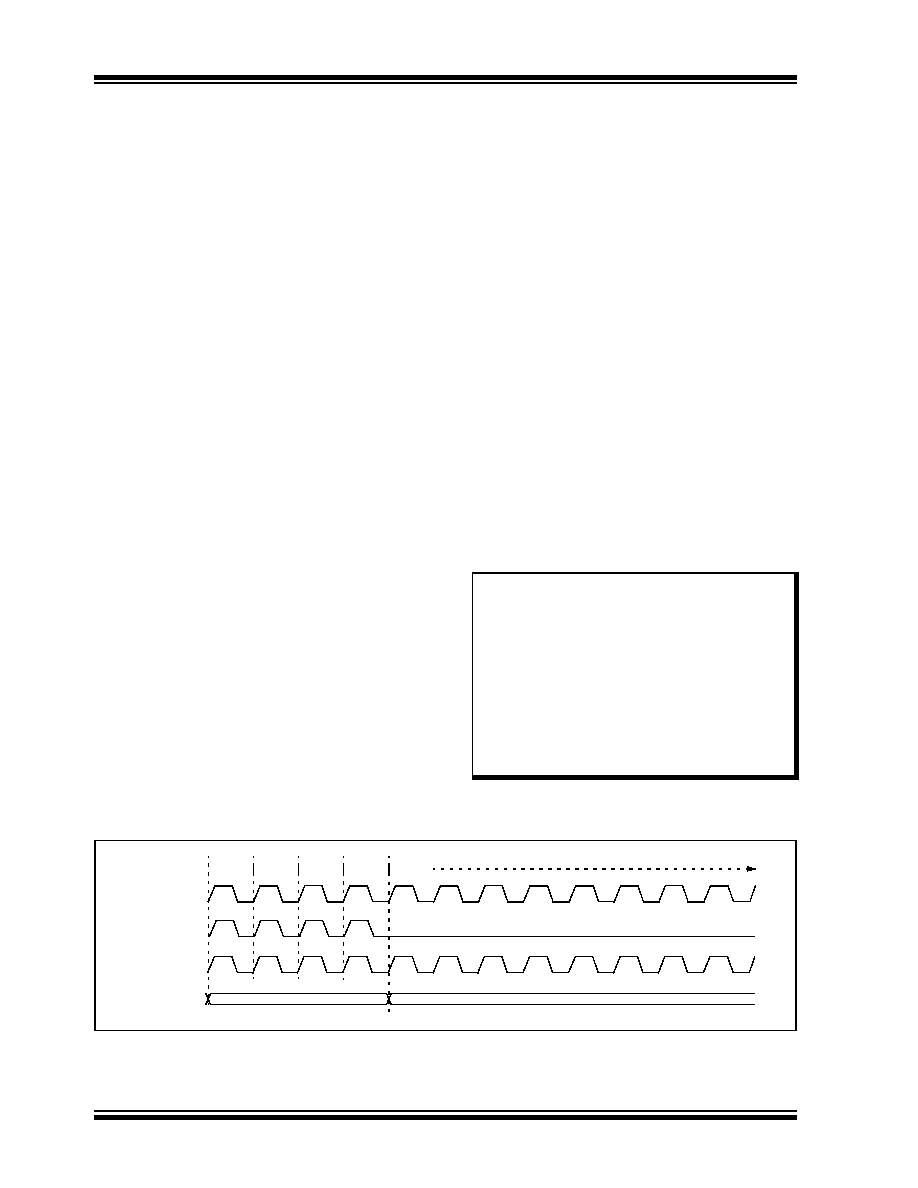
Although the CPU is disabled, the peripherals continue
to be clocked from the primary clock source specified
by the FOSC<1:0> Configuration bits. The OSTS bit
remains set (see Figure 4-7).
When a wake event occurs, the CPU is clocked from the
primary clock source. After the wake-up, the OSTS bit
remains set. The IDLEN and SCS bits are not affected
by the wake-up (see Figure 4-8).
4.4.2
SEC_IDLE MODE
In SEC_IDLE mode, the CPU is disabled but the
peripherals continue to be clocked from the Timer1
oscillator. This mode is entered from SEC_RUN by set-
ting the IDLEN bit and executing a SLEEP instruction. If
the device is in another Run mode, set IDLEN first, then
set SCS<1:0> to ‘01’ and execute SLEEP. When the
clock source is switched to the Timer1 oscillator, the
primary oscillator is shut down (unless some other
peripheral is still requesting it), the OSTS bit is cleared
and the T1RUN bit is set.
When a wake event occurs, the peripherals continue to
be clocked from the Timer1 oscillator. After a wake
event, the CPU begins executing code being clocked
by the Timer1 oscillator. The IDLEN and SCS bits are
not affected by the wake-up; the Timer1 oscillator
continues to run (see Figure 4-8).
FIGURE 4-7:
TRANSITION TIMING FOR ENTRY TO IDLE MODE
Note:
The Timer1 oscillator should already be
running prior to entering SEC_IDLE
mode. If the T1OSCEN bit is not set when
the SLEEP instruction is executed, the
SLEEP
instruction will be ignored and
entry to SEC_IDLE mode will not occur. If
the Timer1 oscillator is enabled, but not
yet running, peripheral clocks will be
delayed until the oscillator has started. In
such situations, initial oscillator operation
is far from stable and unpredictable
operation may result.
Q1
Peripheral
Program
PC
PC + 2
OSC1
Q3
Q4
Q1
CPU Clock
Clock
Counter
Q2
相关PDF资料 |
PDF描述 |
|---|---|
| ATMEGA128L-8AC | IC AVR MCU 128K 8MHZ LV 64-TQFP |
| ATMEGA128-16AI | IC AVR MCU 128K 16MHZ 64-TQFP |
| PIC24EP64GP202-I/SS | MCU 16BIT 64KB FLASH 28SSOP |
| ATMEGA128-16AC | IC AVR MCU 128K 16MHZ 64-TQFP |
| PIC18LF26J50-I/ML | IC PIC MCU FLASH 64K 2V 28-QFN |
相关代理商/技术参数 |
参数描述 |
|---|---|
| PIC18F45J50T-I/ML | 功能描述:8位微控制器 -MCU Full Spd USB 32KB 4KBRAM nanoWatt RoHS:否 制造商:Silicon Labs 核心:8051 处理器系列:C8051F39x 数据总线宽度:8 bit 最大时钟频率:50 MHz 程序存储器大小:16 KB 数据 RAM 大小:1 KB 片上 ADC:Yes 工作电源电压:1.8 V to 3.6 V 工作温度范围:- 40 C to + 105 C 封装 / 箱体:QFN-20 安装风格:SMD/SMT |
| PIC18F45J50T-I/PT | 功能描述:8位微控制器 -MCU Full Spd USB 32KB 4KBRAM nanoWatt RoHS:否 制造商:Silicon Labs 核心:8051 处理器系列:C8051F39x 数据总线宽度:8 bit 最大时钟频率:50 MHz 程序存储器大小:16 KB 数据 RAM 大小:1 KB 片上 ADC:Yes 工作电源电压:1.8 V to 3.6 V 工作温度范围:- 40 C to + 105 C 封装 / 箱体:QFN-20 安装风格:SMD/SMT |
| PIC18F45K20-E/ML | 功能描述:8位微控制器 -MCU 32KB Flash 1536B RAM 25 I/O 8B RoHS:否 制造商:Silicon Labs 核心:8051 处理器系列:C8051F39x 数据总线宽度:8 bit 最大时钟频率:50 MHz 程序存储器大小:16 KB 数据 RAM 大小:1 KB 片上 ADC:Yes 工作电源电压:1.8 V to 3.6 V 工作温度范围:- 40 C to + 105 C 封装 / 箱体:QFN-20 安装风格:SMD/SMT |
| PIC18F45K20-E/MV | 功能描述:8位微控制器 -MCU 32KB FL 1536b RAM 8b Familynanowatt XLP RoHS:否 制造商:Silicon Labs 核心:8051 处理器系列:C8051F39x 数据总线宽度:8 bit 最大时钟频率:50 MHz 程序存储器大小:16 KB 数据 RAM 大小:1 KB 片上 ADC:Yes 工作电源电压:1.8 V to 3.6 V 工作温度范围:- 40 C to + 105 C 封装 / 箱体:QFN-20 安装风格:SMD/SMT |
| PIC18F45K20-E/P | 功能描述:8位微控制器 -MCU 32KB Flash 1536B RAM 25 I/O 8B RoHS:否 制造商:Silicon Labs 核心:8051 处理器系列:C8051F39x 数据总线宽度:8 bit 最大时钟频率:50 MHz 程序存储器大小:16 KB 数据 RAM 大小:1 KB 片上 ADC:Yes 工作电源电压:1.8 V to 3.6 V 工作温度范围:- 40 C to + 105 C 封装 / 箱体:QFN-20 安装风格:SMD/SMT |
发布紧急采购,3分钟左右您将得到回复。