- 您现在的位置:买卖IC网 > PDF目录3857 > PIC18F45J50-I/ML (Microchip Technology)IC PIC MCU FLASH 32K 2V 44-QFN PDF资料下载
参数资料
| 型号: | PIC18F45J50-I/ML |
| 厂商: | Microchip Technology |
| 文件页数: | 37/164页 |
| 文件大小: | 0K |
| 描述: | IC PIC MCU FLASH 32K 2V 44-QFN |
| 产品培训模块: | XLP Deep Sleep Mode PIC18 J Series MCU Overview 8-bit PIC® Microcontroller Portfolio |
| 标准包装: | 45 |
| 系列: | PIC® XLP™ 18F |
| 核心处理器: | PIC |
| 芯体尺寸: | 8-位 |
| 速度: | 48MHz |
| 连通性: | I²C,SPI,UART/USART,USB |
| 外围设备: | 欠压检测/复位,DMA,POR,PWM,WDT |
| 输入/输出数: | 34 |
| 程序存储器容量: | 32KB(16K x 16) |
| 程序存储器类型: | 闪存 |
| RAM 容量: | 3.8K x 8 |
| 电压 - 电源 (Vcc/Vdd): | 2.15 V ~ 3.6 V |
| 数据转换器: | A/D 13x10b |
| 振荡器型: | 内部 |
| 工作温度: | -40°C ~ 85°C |
| 封装/外壳: | 44-VQFN 裸露焊盘 |
| 包装: | 管件 |
| 产品目录页面: | 657 (CN2011-ZH PDF) |
| 配用: | AC164322-ND - MODULE SOCKET MPLAB PM3 28/44QFN |
第1页第2页第3页第4页第5页第6页第7页第8页第9页第10页第11页第12页第13页第14页第15页第16页第17页第18页第19页第20页第21页第22页第23页第24页第25页第26页第27页第28页第29页第30页第31页第32页第33页第34页第35页第36页当前第37页第38页第39页第40页第41页第42页第43页第44页第45页第46页第47页第48页第49页第50页第51页第52页第53页第54页第55页第56页第57页第58页第59页第60页第61页第62页第63页第64页第65页第66页第67页第68页第69页第70页第71页第72页第73页第74页第75页第76页第77页第78页第79页第80页第81页第82页第83页第84页第85页第86页第87页第88页第89页第90页第91页第92页第93页第94页第95页第96页第97页第98页第99页第100页第101页第102页第103页第104页第105页第106页第107页第108页第109页第110页第111页第112页第113页第114页第115页第116页第117页第118页第119页第120页第121页第122页第123页第124页第125页第126页第127页第128页第129页第130页第131页第132页第133页第134页第135页第136页第137页第138页第139页第140页第141页第142页第143页第144页第145页第146页第147页第148页第149页第150页第151页第152页第153页第154页第155页第156页第157页第158页第159页第160页第161页第162页第163页第164页
2011 Microchip Technology Inc.
DS39931D-page 131
PIC18F46J50 FAMILY
10.0
I/O PORTS
Depending on the device selected and features
enabled, there are up to five ports available. Some pins
of the I/O ports are multiplexed with an alternate
function from the peripheral features on the device. In
general, when a peripheral is enabled, that pin may not
be used as a general purpose I/O pin.
Each port has three registers for its operation. These
registers are:
TRIS register (Data Direction register)
PORT register (reads the levels on the pins of the
device)
LAT register (Data Latch)
Pins that are multiplexed with analog functionality (ANx
pins) also have ANCON register bits associated with
them.
The TRISx registers control which pins should be con-
figured as digital outputs (output buffer enabled) and
which pins should be left high-impedance. Writing ‘0’ to
a TRIS bit configures the specified pin as a digital out-
put. Writing a ‘1’ to a TRIS bit disables the output driver,
so the pin can be used as a digital or analog input. This
can be easily remembered by observing that ‘0’ is sim-
ilar to the letter, O (as in Output), and that ‘1’ is similar
to the letter, I (as in Input).
The PORTx registers can be used to read the logic level
externally presented on pins that have been configured
as digital inputs. If a pin is configured as a digital input,
the corresponding port bit will be read as ‘1’ if the exter-
nally applied voltage is greater than the VIH level for that
pin. If the externally applied voltage is below VIL, then
the PORTx bit will read as ‘0’. If the I/O pin is multiplexed
with analog functionality (an ANx pin), then the corre-
sponding PCFG bit, in the appropriate ANCONx register,
must also be set, in order to correctly read the externally
applied voltage on the pin. See the following information
regarding the ANCONx registers.
If the application firmware writes to a PORTx register,
this will cause the corresponding LATx register to be
updated. It is usually not recommended to perform
read-modify-write instructions (ex: BTG, BSF, BCF) on a
PORTx register. If the application firmware wishes to
change the output state of a pin that has been
configured as a digital output (TRIS bit = 0), it is
recommended that the firmware use the corresponding
LATx register instead.
The LATx registers hold the digital value that is output
onto a pin when the pin has been configured as a digital
output (TRIS bit = 0). Writing a ‘1’ to the LATx bit will
drive the output pin to the logic high output state.
Similarly, writing a ‘0’ to the LAT bit will drive the output
pin to a logic low output state. It is safe to perform all
types of read, write and read-modify-write instructions
on the LATx registers.
The ANCONx registers are used to configure pins with
ANx analog functionality for either Digital Input or Analog
Input mode. Setting a PCFG bit in an ANCONx register
enables the digital input buffer, allowing reads from the
PORTx register to correctly reflect the externally applied
voltage on the digital input pin. If the PCFG bit is clear,
the digital input buffer is disabled, to eliminate CMOS
input buffer cross conduction currents, when a mid-VDD
scale analog voltage is applied to the pin. This allows
analog input voltages (between VDD and VSS) to be
applied to the pin without increasing the current con-
sumption of the device. If the appropriate PCFG bit in the
ANCONx register is not set, this will cause the PORTx
register bit for that pin to read as ‘0’, regardless of the
actually applied external voltage.
At power-up, the default state of the ANCONx registers
is to configure the ANx pins for Analog mode (digital
input buffer off). Therefore, to use ANx pins as digital
inputs, the application firmware must first update the
ANCONx register(s). See Section 21.0 “10-bit Ana-
for more
details regarding the ANCONx registers.
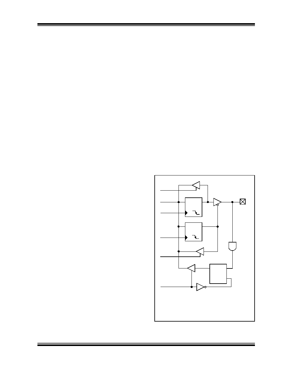
Figure 10-1 displays a simplified model of a generic I/O
port, without the interfaces to other peripherals.
FIGURE 10-1:
GENERIC I/O PORT
OPERATION
Data
Bus
WR LAT
WR TRIS
RD PORT
Data Latch
TRIS Latch
RD TRIS
Input
Buffer
I/O Pin(1)
Q
D
CK
Q
D
CK
EN
QD
EN
RD LAT
or PORT
Note 1:
I/O pins without 5.5V tolerance have diode
protection to VDD and VSS. I/O pins with
5.5V tolerance have diode protection from
Vss.
相关PDF资料 |
PDF描述 |
|---|---|
| ATMEGA128L-8AC | IC AVR MCU 128K 8MHZ LV 64-TQFP |
| ATMEGA128-16AI | IC AVR MCU 128K 16MHZ 64-TQFP |
| PIC24EP64GP202-I/SS | MCU 16BIT 64KB FLASH 28SSOP |
| ATMEGA128-16AC | IC AVR MCU 128K 16MHZ 64-TQFP |
| PIC18LF26J50-I/ML | IC PIC MCU FLASH 64K 2V 28-QFN |
相关代理商/技术参数 |
参数描述 |
|---|---|
| PIC18F45J50T-I/ML | 功能描述:8位微控制器 -MCU Full Spd USB 32KB 4KBRAM nanoWatt RoHS:否 制造商:Silicon Labs 核心:8051 处理器系列:C8051F39x 数据总线宽度:8 bit 最大时钟频率:50 MHz 程序存储器大小:16 KB 数据 RAM 大小:1 KB 片上 ADC:Yes 工作电源电压:1.8 V to 3.6 V 工作温度范围:- 40 C to + 105 C 封装 / 箱体:QFN-20 安装风格:SMD/SMT |
| PIC18F45J50T-I/PT | 功能描述:8位微控制器 -MCU Full Spd USB 32KB 4KBRAM nanoWatt RoHS:否 制造商:Silicon Labs 核心:8051 处理器系列:C8051F39x 数据总线宽度:8 bit 最大时钟频率:50 MHz 程序存储器大小:16 KB 数据 RAM 大小:1 KB 片上 ADC:Yes 工作电源电压:1.8 V to 3.6 V 工作温度范围:- 40 C to + 105 C 封装 / 箱体:QFN-20 安装风格:SMD/SMT |
| PIC18F45K20-E/ML | 功能描述:8位微控制器 -MCU 32KB Flash 1536B RAM 25 I/O 8B RoHS:否 制造商:Silicon Labs 核心:8051 处理器系列:C8051F39x 数据总线宽度:8 bit 最大时钟频率:50 MHz 程序存储器大小:16 KB 数据 RAM 大小:1 KB 片上 ADC:Yes 工作电源电压:1.8 V to 3.6 V 工作温度范围:- 40 C to + 105 C 封装 / 箱体:QFN-20 安装风格:SMD/SMT |
| PIC18F45K20-E/MV | 功能描述:8位微控制器 -MCU 32KB FL 1536b RAM 8b Familynanowatt XLP RoHS:否 制造商:Silicon Labs 核心:8051 处理器系列:C8051F39x 数据总线宽度:8 bit 最大时钟频率:50 MHz 程序存储器大小:16 KB 数据 RAM 大小:1 KB 片上 ADC:Yes 工作电源电压:1.8 V to 3.6 V 工作温度范围:- 40 C to + 105 C 封装 / 箱体:QFN-20 安装风格:SMD/SMT |
| PIC18F45K20-E/P | 功能描述:8位微控制器 -MCU 32KB Flash 1536B RAM 25 I/O 8B RoHS:否 制造商:Silicon Labs 核心:8051 处理器系列:C8051F39x 数据总线宽度:8 bit 最大时钟频率:50 MHz 程序存储器大小:16 KB 数据 RAM 大小:1 KB 片上 ADC:Yes 工作电源电压:1.8 V to 3.6 V 工作温度范围:- 40 C to + 105 C 封装 / 箱体:QFN-20 安装风格:SMD/SMT |
发布紧急采购,3分钟左右您将得到回复。