- 您现在的位置:买卖IC网 > PDF目录378055 > PM73121-RI (PMC-SIERRA INC) AAL1 Segmentation And Reassembly Processor PDF资料下载
参数资料
| 型号: | PM73121-RI |
| 厂商: | PMC-SIERRA INC |
| 元件分类: | 数字传输电路 |
| 英文描述: | AAL1 Segmentation And Reassembly Processor |
| 中文描述: | ATM SEGMENTATION AND REASSEMBLY DEVICE, PQFP240 |
| 封装: | QFP-240 |
| 文件页数: | 122/223页 |
| 文件大小: | 2300K |
| 代理商: | PM73121-RI |
第1页第2页第3页第4页第5页第6页第7页第8页第9页第10页第11页第12页第13页第14页第15页第16页第17页第18页第19页第20页第21页第22页第23页第24页第25页第26页第27页第28页第29页第30页第31页第32页第33页第34页第35页第36页第37页第38页第39页第40页第41页第42页第43页第44页第45页第46页第47页第48页第49页第50页第51页第52页第53页第54页第55页第56页第57页第58页第59页第60页第61页第62页第63页第64页第65页第66页第67页第68页第69页第70页第71页第72页第73页第74页第75页第76页第77页第78页第79页第80页第81页第82页第83页第84页第85页第86页第87页第88页第89页第90页第91页第92页第93页第94页第95页第96页第97页第98页第99页第100页第101页第102页第103页第104页第105页第106页第107页第108页第109页第110页第111页第112页第113页第114页第115页第116页第117页第118页第119页第120页第121页当前第122页第123页第124页第125页第126页第127页第128页第129页第130页第131页第132页第133页第134页第135页第136页第137页第138页第139页第140页第141页第142页第143页第144页第145页第146页第147页第148页第149页第150页第151页第152页第153页第154页第155页第156页第157页第158页第159页第160页第161页第162页第163页第164页第165页第166页第167页第168页第169页第170页第171页第172页第173页第174页第175页第176页第177页第178页第179页第180页第181页第182页第183页第184页第185页第186页第187页第188页第189页第190页第191页第192页第193页第194页第195页第196页第197页第198页第199页第200页第201页第202页第203页第204页第205页第206页第207页第208页第209页第210页第211页第212页第213页第214页第215页第216页第217页第218页第219页第220页第221页第222页第223页
PMC-Sierra, Inc.
PM73121AAL1gator II
L
PMC-980620
,VVXH
AAL1 SAR Processor
Data Sheet
35235,(7$5<$1'&21),'(17,$/7230&6,(55$,1&$1')25,76&86720(56,17(51$/86(
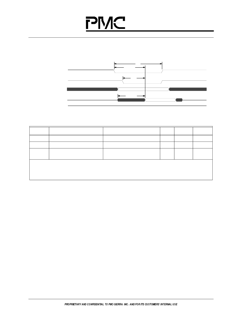
Figure 70 shows the timing information for all RAM read cycles.
6.5.2
Microprocessor Timing
Microprocessor accesses are controlled by the AAL1gator II. To properly access the
AAL1gator II and the external memory, the AAL1gator II must be supported with a tristatable
address buffer and a bidirectional tristatable data latch.
6.5.2.1
Microprocessor RAM Write Cycle Timing
Figure 71 on page 107
shows the timing for a microprocessor-initiated write cycle. It shows the
2-cycle write operation occurring immediately after a non-processor read cycle. RAM writing is
not honored if higher priority internal functions request the memory, or the holdoff from a previ-
ous microprocessor transfer has not expired. /PROC_CS and /PROC_WR are double sampled (1
and 2) with the rising edge of SYS_CLK, and at (3) ADDR17 is sampled to distinguish between a
command register write and a RAM write.
Figure 70.
RAM Read Cycle Timing
Symbol
Parameter
Signals
Min
Max
Unit
Toe
RAM output enable delay
MEM_DATA
0
7
ns
Trc
Read cycle
/MEM_CS
Tp-2
ns
Trdacc
Read access time
MEM_DATA, /MEM_CS, /MEM_
ADDR
16 + Tsc
ns
NOTES:
Tsc = (1
÷
Fc) - (1
÷
38.87 MHz). For Fc and Tp values, see
Figure 80 on page 119
.
Test conditions are: /MEM_WE(0) and /MEM_WE(1) at 15 pF; and MEM_DATA, SP_DATA_EN, SP_
DATA_CLK, SP_DATA_DIR, and /MEM_CS at 30 pF; MEM_ADDR and SP_ADDR_EN at 40 pF.
All outputs are measured at 1.5 V, -40 to 85
°
C, 4.75 - 5.25 V.
Trc
Trdacc
Toe
Trdacc
/MEM_CS(o)
/MEM_OE(o)
MEM_ADDR(io)
MEM_DATA(io)
/MEM_WE(o)
相关PDF资料 |
PDF描述 |
|---|---|
| PM73122 | 32 LINK CES/DBCES AAL1 SAR PROCESSOR |
| PM73122-BI | 32 LINK CES/DBCES AAL1 SAR PROCESSOR |
| PM73123 | 8 LINK CES/DBCES AAL1 SAR |
| PM73123-PI | 8 LINK CES/DBCES AAL1 SAR |
| PM73124 | 4 Link CES/DBCES AAL1 SAR |
相关代理商/技术参数 |
参数描述 |
|---|---|
| PM73122 | 制造商:PMC 制造商全称:PMC 功能描述:32 LINK CES/DBCES AAL1 SAR PROCESSOR |
| PM73122-BI | 制造商:PMC 制造商全称:PMC 功能描述:32 LINK CES/DBCES AAL1 SAR PROCESSOR |
| PM73122-BIP | 制造商:PMC-Sierra 功能描述:AAL1GATOR32 EOL270906 |
| PM73122-BI-P | 制造商:PMC-Sierra 功能描述: |
发布紧急采购,3分钟左右您将得到回复。