- 您现在的位置:买卖IC网 > PDF目录378055 > PM73121-RI (PMC-SIERRA INC) AAL1 Segmentation And Reassembly Processor PDF资料下载
参数资料
| 型号: | PM73121-RI |
| 厂商: | PMC-SIERRA INC |
| 元件分类: | 数字传输电路 |
| 英文描述: | AAL1 Segmentation And Reassembly Processor |
| 中文描述: | ATM SEGMENTATION AND REASSEMBLY DEVICE, PQFP240 |
| 封装: | QFP-240 |
| 文件页数: | 127/223页 |
| 文件大小: | 2300K |
| 代理商: | PM73121-RI |
第1页第2页第3页第4页第5页第6页第7页第8页第9页第10页第11页第12页第13页第14页第15页第16页第17页第18页第19页第20页第21页第22页第23页第24页第25页第26页第27页第28页第29页第30页第31页第32页第33页第34页第35页第36页第37页第38页第39页第40页第41页第42页第43页第44页第45页第46页第47页第48页第49页第50页第51页第52页第53页第54页第55页第56页第57页第58页第59页第60页第61页第62页第63页第64页第65页第66页第67页第68页第69页第70页第71页第72页第73页第74页第75页第76页第77页第78页第79页第80页第81页第82页第83页第84页第85页第86页第87页第88页第89页第90页第91页第92页第93页第94页第95页第96页第97页第98页第99页第100页第101页第102页第103页第104页第105页第106页第107页第108页第109页第110页第111页第112页第113页第114页第115页第116页第117页第118页第119页第120页第121页第122页第123页第124页第125页第126页当前第127页第128页第129页第130页第131页第132页第133页第134页第135页第136页第137页第138页第139页第140页第141页第142页第143页第144页第145页第146页第147页第148页第149页第150页第151页第152页第153页第154页第155页第156页第157页第158页第159页第160页第161页第162页第163页第164页第165页第166页第167页第168页第169页第170页第171页第172页第173页第174页第175页第176页第177页第178页第179页第180页第181页第182页第183页第184页第185页第186页第187页第188页第189页第190页第191页第192页第193页第194页第195页第196页第197页第198页第199页第200页第201页第202页第203页第204页第205页第206页第207页第208页第209页第210页第211页第212页第213页第214页第215页第216页第217页第218页第219页第220页第221页第222页第223页
PMC-Sierra, Inc.
PM73121AAL1gator II
L
PMC-980620
,VVXH
AAL1 SAR Processor
Data Sheet
35235,(7$5<$1'&21),'(17,$/7230&6,(55$,1&$1')25,76&86720(56,17(51$/86(
NOTE: Taa is dependent on the HOLDOFF signal. If HOLDOFF is not asserted when the
access begins, Taa will be a maximum of six SYS_CLK periods. If the access occurs
immediately after another access, then Taa will be 24 to 30 SYS_CLK periods. Refer
to
section 6.5.3 “Microprocessor Holdoff Timing” on page 116
for a description of
the HOLDOFF activity.
6.5.2.3
Microprocessor Write Command Register Timing
Figure 73 on page 112
shows the write command register timing. Writing to the internal com-
mand register is not honored if higher priority internal functions request the memory, or if the
holdoff from a previous microprocessor transfer has not expired.
/PROC_CS and /PROC_WR are double sampled (1 and 2) at the rising edge of SYS_CLK, and at
(3) ADDR17 is sampled to distinguish between a command register write and a RAM write.
As long as HOLDOFF is not high, /SP_ADD_EN, /SP_DATA_EN, and SP_DATA_DIR are acti-
vated at the next clock cycle (3), allowing the microprocessor address and data to pass through the
address and data buffer to the AAL1gator II. The /SP_ADD_EN and the /SP_DATA_EN signals
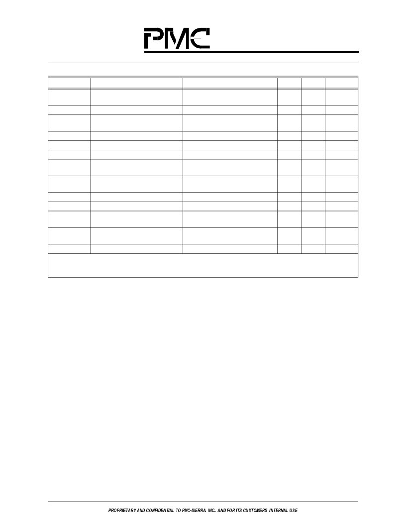
Tq
Clock-to-output delay
SP_DATA_CLK,/MEM_OE
(deactivate)
/MEM_CS
MEM_OE (activate)
2
15
ns
Tq
Clock-to-output delay
Clock-to-output delay for activation
of /MEM_OE
Address setup to SYS_CLK
Address enable delay
Address setup to SP_DATA_CLK*
Data enable delay from /PROC_CS
and /PROC_RD
/PROC_CS deassertion to /PROC_
ACK deassertion
Data setup to SP_DATA_CLK*
Data hold from SP_DATA_CLK*
SP_DATA_CLK high to
/SP_ADD_EN high
MEM_ADDR hold time from SP_
DATA_CLK*
Z state setup-to-clock
* These parameters are dependent on external components and assume that the requirements from
Table 26 on page 195
are
met.
** These parameters are typical only.
2
2
18
25
ns
ns
Tqmoe
Tasu17
Taed
Tasu
Tded
ADDR17
/SP_ADD_EN
MEM_ADDR, SP_DATA_CLK
/SP_DATA_EN, /PROC_CS,
/PROC_RD
/PROC_ACK
2
5
26
2**
ns
ns
ns
ns
20
15**
Tcea
2
15
ns
Tdsu
Tdh
Tcaen
MEM_DATA
MEM_DATA, SP_DATA_CLK
SP_DATA_CLK, /SP_ADD_EN
11
3
0
ns
ns
ns
Tah
MEM_ADD, SP_DATA_CLK
1
ns
Tzsu
MEM_ADDR
3**
ns
Symbol
Parameter
Signals
Min
Max
Unit
相关PDF资料 |
PDF描述 |
|---|---|
| PM73122 | 32 LINK CES/DBCES AAL1 SAR PROCESSOR |
| PM73122-BI | 32 LINK CES/DBCES AAL1 SAR PROCESSOR |
| PM73123 | 8 LINK CES/DBCES AAL1 SAR |
| PM73123-PI | 8 LINK CES/DBCES AAL1 SAR |
| PM73124 | 4 Link CES/DBCES AAL1 SAR |
相关代理商/技术参数 |
参数描述 |
|---|---|
| PM73122 | 制造商:PMC 制造商全称:PMC 功能描述:32 LINK CES/DBCES AAL1 SAR PROCESSOR |
| PM73122-BI | 制造商:PMC 制造商全称:PMC 功能描述:32 LINK CES/DBCES AAL1 SAR PROCESSOR |
| PM73122-BIP | 制造商:PMC-Sierra 功能描述:AAL1GATOR32 EOL270906 |
| PM73122-BI-P | 制造商:PMC-Sierra 功能描述: |
发布紧急采购,3分钟左右您将得到回复。