- 您现在的位置:买卖IC网 > PDF目录368262 > PSD835G2V-A-20J (意法半导体) Configurable Memory System on a Chip for 8-Bit Microcontrollers PDF资料下载
参数资料
| 型号: | PSD835G2V-A-20J |
| 厂商: | 意法半导体 |
| 英文描述: | Configurable Memory System on a Chip for 8-Bit Microcontrollers |
| 中文描述: | 在8片位微控制器可配置存储系统 |
| 文件页数: | 34/110页 |
| 文件大小: | 570K |
| 代理商: | PSD835G2V-A-20J |
第1页第2页第3页第4页第5页第6页第7页第8页第9页第10页第11页第12页第13页第14页第15页第16页第17页第18页第19页第20页第21页第22页第23页第24页第25页第26页第27页第28页第29页第30页第31页第32页第33页当前第34页第35页第36页第37页第38页第39页第40页第41页第42页第43页第44页第45页第46页第47页第48页第49页第50页第51页第52页第53页第54页第55页第56页第57页第58页第59页第60页第61页第62页第63页第64页第65页第66页第67页第68页第69页第70页第71页第72页第73页第74页第75页第76页第77页第78页第79页第80页第81页第82页第83页第84页第85页第86页第87页第88页第89页第90页第91页第92页第93页第94页第95页第96页第97页第98页第99页第100页第101页第102页第103页第104页第105页第106页第107页第108页第109页第110页
PSD835G2
PSD8XX Family
33
The
PSD835G2
Functional
Blocks
(cont.)
9.2 PLDs
The PLDs bring programmable logic functionality to the PSD835G2. After specifying the
logic for the PLDs in PSDsoft, the logic is programmed into the device and available upon
power-up.
The PSD835G2 contains two PLDs: the Decode PLD (DPLD), and the Complex PLD
(CPLD). The PLDs are briefly discussed in the next few paragraphs, and in more detail in
sections 9.2.1 and 9.2.2. Figure 10 shows the configuration of the PLDs.
The DPLD performs address decoding for internal components, such as memory,
registers, and I/O port selects.
The CPLD can be used for logic functions, such as loadable counters and shift registers,
state machines, and encoding and decoding logic. These logic functions can be
constructed using the 16 Output Micro
Cells (OMCs), 24 Input Micro
Cells (IMCs), and
the AND array. The CPLD can also be used to generate external chip selects.
The AND array is used to form product terms. These product terms are specified using
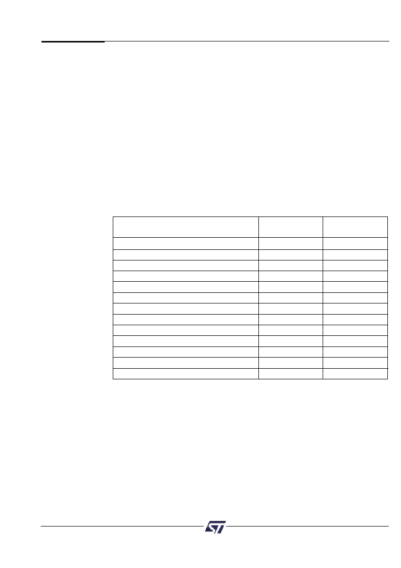
PSDsoft. An Input Bus consisting of 82 signals is connected to the PLDs. The signals are
shown in Table 12.
Input Source
Input Name
Number
of Signals
MCU Address Bus
MCU Control Signals
Reset
Power Down
Port A Input Micro
Cells
Port B Input Micro
Cells
Port C Input Micro
Cells
Port D Inputs
Port F Inputs
Page Register
Micro
Cell A Feedback
Micro
Cell B Feedback
Flash Programming Status Bit
A[15:0]
*
CNTL[2:0]
RST
PDN
PA[7-0]
PB[7-0]
PC[7-0]
PD[3:0]
PF[7:0]
PGR(7:0)
MCELLA.FB[7:0]
MCELLB.FB[7:0]
Rdy/Bsy
16
3
1
1
8
8
8
4
8
8
8
8
1
Table 12. DPLD and CPLD Inputs
NOTE:
The address inputs are A[19:4] in 80C51XA mode.
The Turbo Bit
The PLDs in the PSD835G2 can minimize power consumption by switching to standby
when inputs remain unchanged for an extended time of about 70 ns. Setting the Turbo
mode bit to off (Bit 3 of the PMMR0 register) automatically places the PLDs into standby if
no inputs are changing. Turbo-off mode increases propagation delays while reducing
power consumption. Refer to the Power Management Unit section on how to set the Turbo
Bit. Additionally, five bits are available in the PMMR2 register to block MCU control signals
from entering the PLDs. This reduces power consumption and can be used only when
these MCU control signals are not used in PLD logic equations.
相关PDF资料 |
PDF描述 |
|---|---|
| PSD835G2V-A-20JI | Configurable Memory System on a Chip for 8-Bit Microcontrollers |
| PSD835G2V-A-20M | Configurable Memory System on a Chip for 8-Bit Microcontrollers |
| PSD835G2V-A-20MI | Configurable Memory System on a Chip for 8-Bit Microcontrollers |
| PSD835G2V-A-20U | Configurable Memory System on a Chip for 8-Bit Microcontrollers |
| PSD835G2V-A-20UI | Configurable Memory System on a Chip for 8-Bit Microcontrollers |
相关代理商/技术参数 |
参数描述 |
|---|---|
| PSD853F2-70J | 功能描述:SPLD - 简单可编程逻辑器件 5.0V 1M 70ns RoHS:否 制造商:Texas Instruments 逻辑系列:TICPAL22V10Z 大电池数量:10 最大工作频率:66 MHz 延迟时间:25 ns 工作电源电压:4.75 V to 5.25 V 电源电流:100 uA 最大工作温度:+ 75 C 最小工作温度:0 C 安装风格:Through Hole 封装 / 箱体:DIP-24 |
| PSD853F2-70M | 功能描述:CPLD - 复杂可编程逻辑器件 5.0V 1M 70ns RoHS:否 制造商:Lattice 系列: 存储类型:EEPROM 大电池数量:128 最大工作频率:333 MHz 延迟时间:2.7 ns 可编程输入/输出端数量:64 工作电源电压:3.3 V 最大工作温度:+ 90 C 最小工作温度:0 C 封装 / 箱体:TQFP-100 |
| PSD853F2-90J | 功能描述:CPLD - 复杂可编程逻辑器件 5.0V 1M 90ns RoHS:否 制造商:Lattice 系列: 存储类型:EEPROM 大电池数量:128 最大工作频率:333 MHz 延迟时间:2.7 ns 可编程输入/输出端数量:64 工作电源电压:3.3 V 最大工作温度:+ 90 C 最小工作温度:0 C 封装 / 箱体:TQFP-100 |
| PSD853F2-90JI | 功能描述:CPLD - 复杂可编程逻辑器件 5.0V 1M 90ns RoHS:否 制造商:Lattice 系列: 存储类型:EEPROM 大电池数量:128 最大工作频率:333 MHz 延迟时间:2.7 ns 可编程输入/输出端数量:64 工作电源电压:3.3 V 最大工作温度:+ 90 C 最小工作温度:0 C 封装 / 箱体:TQFP-100 |
| PSD853F2-90M | 功能描述:CPLD - 复杂可编程逻辑器件 5.0V 1M 90ns RoHS:否 制造商:Lattice 系列: 存储类型:EEPROM 大电池数量:128 最大工作频率:333 MHz 延迟时间:2.7 ns 可编程输入/输出端数量:64 工作电源电压:3.3 V 最大工作温度:+ 90 C 最小工作温度:0 C 封装 / 箱体:TQFP-100 |
发布紧急采购,3分钟左右您将得到回复。