- 您现在的位置:买卖IC网 > PDF目录368262 > PSD835G2V-A-20J (意法半导体) Configurable Memory System on a Chip for 8-Bit Microcontrollers PDF资料下载
参数资料
| 型号: | PSD835G2V-A-20J |
| 厂商: | 意法半导体 |
| 英文描述: | Configurable Memory System on a Chip for 8-Bit Microcontrollers |
| 中文描述: | 在8片位微控制器可配置存储系统 |
| 文件页数: | 42/110页 |
| 文件大小: | 570K |
| 代理商: | PSD835G2V-A-20J |
第1页第2页第3页第4页第5页第6页第7页第8页第9页第10页第11页第12页第13页第14页第15页第16页第17页第18页第19页第20页第21页第22页第23页第24页第25页第26页第27页第28页第29页第30页第31页第32页第33页第34页第35页第36页第37页第38页第39页第40页第41页当前第42页第43页第44页第45页第46页第47页第48页第49页第50页第51页第52页第53页第54页第55页第56页第57页第58页第59页第60页第61页第62页第63页第64页第65页第66页第67页第68页第69页第70页第71页第72页第73页第74页第75页第76页第77页第78页第79页第80页第81页第82页第83页第84页第85页第86页第87页第88页第89页第90页第91页第92页第93页第94页第95页第96页第97页第98页第99页第100页第101页第102页第103页第104页第105页第106页第107页第108页第109页第110页
PSD835G2
PSD8XX Family
41
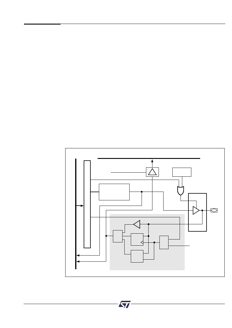
9.2.2.6 Input Micro
Cells (IMCs)
The CPLD has 24 IMCs, one for each pin on Ports A, B, and C. The architecture of the IMC
is shown in Figure 14. The IMCs are individually configurable, and can be used as a latch,
register, or to pass incoming Port signals prior to driving them onto the PLD input bus. The
outputs of the IMCs can be read by the microcontroller through the internal data bus.
The enable for the latch and clock for the register are driven by a multiplexer whose inputs
are a product term from the CPLD AND array or the MCU address strobe (ALE/AS). Each
product term output is used to latch or clock four IMCs. Port inputs 3-0 can be controlled by
one product term and 7-4 by another.
Configurations for the IMCs are specified by PSDsoft. Outputs of the IMCs can be read by
the MCU via the IMC buffer. See the I/O Port section on how to read the IMCs.
IMCs can use the address strobe to latch address bits higher than A15. Any latched
addresses are routed to the PLDs as inputs.
IMCs are particularly useful with handshaking communication applications where two
processors pass data back and forth through a common mailbox. Figure 15 shows a typical
configuration where the Master MCU writes to the Port A Data Out Register. This, in turn,
can be read by the Slave MCU via the activation of the
“
Slave-Read
”
output enable product
term. The Slave can also write to the Port A IMCs and the Master can then read the IMCs
directly. Note that the
“
Slave-Read
”
and
“
Slave-Wr
”
signals are product terms that are
derived from the Slave MCU inputs RD, WR, and Slave_CS.
The
PSD835G2
Functional
Blocks
(cont.)
OUTPUT
MICRO
CELLS A
AND
MICRO
CELL B
PT
PT
FEEDBACK
A
P
PORT
DRIVER
I/O PIN
INTERNAL DATA BUS
DIRECTION
REGISTER
MUX
MUX
ALE/AS
PT
Q
Q
D
D
G
LATCH
INPUT MICRO
CELL
ENABLE (.OE)
D FF
INPUT MICRO
CELL_ RD
Figure 14. Input Micro
Cell
相关PDF资料 |
PDF描述 |
|---|---|
| PSD835G2V-A-20JI | Configurable Memory System on a Chip for 8-Bit Microcontrollers |
| PSD835G2V-A-20M | Configurable Memory System on a Chip for 8-Bit Microcontrollers |
| PSD835G2V-A-20MI | Configurable Memory System on a Chip for 8-Bit Microcontrollers |
| PSD835G2V-A-20U | Configurable Memory System on a Chip for 8-Bit Microcontrollers |
| PSD835G2V-A-20UI | Configurable Memory System on a Chip for 8-Bit Microcontrollers |
相关代理商/技术参数 |
参数描述 |
|---|---|
| PSD853F2-70J | 功能描述:SPLD - 简单可编程逻辑器件 5.0V 1M 70ns RoHS:否 制造商:Texas Instruments 逻辑系列:TICPAL22V10Z 大电池数量:10 最大工作频率:66 MHz 延迟时间:25 ns 工作电源电压:4.75 V to 5.25 V 电源电流:100 uA 最大工作温度:+ 75 C 最小工作温度:0 C 安装风格:Through Hole 封装 / 箱体:DIP-24 |
| PSD853F2-70M | 功能描述:CPLD - 复杂可编程逻辑器件 5.0V 1M 70ns RoHS:否 制造商:Lattice 系列: 存储类型:EEPROM 大电池数量:128 最大工作频率:333 MHz 延迟时间:2.7 ns 可编程输入/输出端数量:64 工作电源电压:3.3 V 最大工作温度:+ 90 C 最小工作温度:0 C 封装 / 箱体:TQFP-100 |
| PSD853F2-90J | 功能描述:CPLD - 复杂可编程逻辑器件 5.0V 1M 90ns RoHS:否 制造商:Lattice 系列: 存储类型:EEPROM 大电池数量:128 最大工作频率:333 MHz 延迟时间:2.7 ns 可编程输入/输出端数量:64 工作电源电压:3.3 V 最大工作温度:+ 90 C 最小工作温度:0 C 封装 / 箱体:TQFP-100 |
| PSD853F2-90JI | 功能描述:CPLD - 复杂可编程逻辑器件 5.0V 1M 90ns RoHS:否 制造商:Lattice 系列: 存储类型:EEPROM 大电池数量:128 最大工作频率:333 MHz 延迟时间:2.7 ns 可编程输入/输出端数量:64 工作电源电压:3.3 V 最大工作温度:+ 90 C 最小工作温度:0 C 封装 / 箱体:TQFP-100 |
| PSD853F2-90M | 功能描述:CPLD - 复杂可编程逻辑器件 5.0V 1M 90ns RoHS:否 制造商:Lattice 系列: 存储类型:EEPROM 大电池数量:128 最大工作频率:333 MHz 延迟时间:2.7 ns 可编程输入/输出端数量:64 工作电源电压:3.3 V 最大工作温度:+ 90 C 最小工作温度:0 C 封装 / 箱体:TQFP-100 |
发布紧急采购,3分钟左右您将得到回复。