- 您现在的位置:买卖IC网 > PDF目录368262 > PSD835G2V-A-20J (意法半导体) Configurable Memory System on a Chip for 8-Bit Microcontrollers PDF资料下载
参数资料
| 型号: | PSD835G2V-A-20J |
| 厂商: | 意法半导体 |
| 英文描述: | Configurable Memory System on a Chip for 8-Bit Microcontrollers |
| 中文描述: | 在8片位微控制器可配置存储系统 |
| 文件页数: | 56/110页 |
| 文件大小: | 570K |
| 代理商: | PSD835G2V-A-20J |
第1页第2页第3页第4页第5页第6页第7页第8页第9页第10页第11页第12页第13页第14页第15页第16页第17页第18页第19页第20页第21页第22页第23页第24页第25页第26页第27页第28页第29页第30页第31页第32页第33页第34页第35页第36页第37页第38页第39页第40页第41页第42页第43页第44页第45页第46页第47页第48页第49页第50页第51页第52页第53页第54页第55页当前第56页第57页第58页第59页第60页第61页第62页第63页第64页第65页第66页第67页第68页第69页第70页第71页第72页第73页第74页第75页第76页第77页第78页第79页第80页第81页第82页第83页第84页第85页第86页第87页第88页第89页第90页第91页第92页第93页第94页第95页第96页第97页第98页第99页第100页第101页第102页第103页第104页第105页第106页第107页第108页第109页第110页
PSD835G2
PSD8XX Family
55
The
PSD835G2
Functional
Blocks
(cont.)
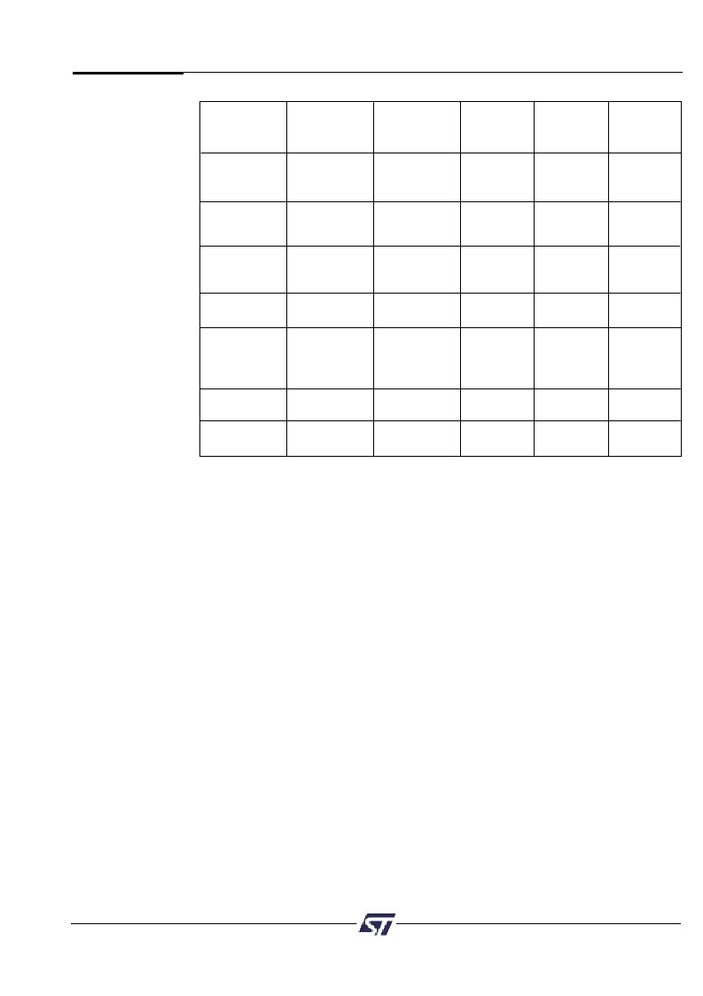
Control
Register
Setting
Direction
Register
Setting
VM
Defined In
PSDsoft
Register
Setting
JTAG
Enable
Mode
Declare
pins only
0
1= output,
0= input
(Note 1)
MCU I/O
(Note 3)
NA
NA
Declare pins
and logic
equations
PLD I/O
NA
(Note 1)
NA
NA
Data Port
(Port F)
Selected for
MCU with
non-mux bus
NA
NA
NA
NA
Address Out
(Port E, F, G)
Declare
pins only
1
1 (Note 1)
NA
NA
Declare pins or
logic equation
Address In
(Port A,B,C,D,F) for input
NA
NA
NA
NA
Micro
Cells
Peripheral I/O
(Port F)
Logic equations
(PSEL0 & 1)
NA
NA
PIO bit =1
NA
JTAG ISP
(Note 2)
Declare pins
only
NA
NA
NA
JTAG_Enable
Table 17. Port Operating Mode Settings
*
NA = Not Applicable
NOTE:
1. The direction of the Port A,B,C, and F pins are controlled by the Direction Register ORed with the
individual output enable product term (.oe) from the CPLD AND array.
2. Any of these three methods will enable JTAG pins on Port E.
3. Control Register setting is not applicable to Ports A, B and C.
9.4.2.1 MCU I/OMode
In the MCU I/O Mode, the microcontroller uses the PSD835G2 ports to expand its own
I/O ports. By setting up the CSIOP space, the ports on the PSD4000 are mapped into the
microcontroller address space. The addresses of the ports are listed in Table 6.
A port pin can be put into MCU I/O mode by writing a ‘0’ to the corresponding bit in the
Control Register (Port E, F and G). The MCU I/O direction may be changed by writing to
the corresponding bit in the Direction Register, or by the output enable product term. See
the subsection on the Direction Register in the “Port Registers” section. When the pin is
configured as an output, the content of the Data Out Register drives the pin. When config-
ured as an input, the microcontroller can read the port input through the Data In buffer.
See Figure 22.
Ports A, B and C do not have Control Registers, and are in MCU I/O mode by default.
They can be used for PLD I/O if they are specified in PSDsoft.
9.4.2.2 PLD I/OMode
The PLD I/O Mode uses a port as an input to the CPLD’s Input Micro
Cells, and/or as an
output from the CPLD’s Output Micro
Cells. The output can be tri-stated with a control
signal. This output enable control signal can be defined by a product term from the PLD, or
by setting the corresponding bit in the Direction Register to ‘0’. The corresponding bit in the
Direction Register must not be set to ‘1’ if the pin is defined as a PLD input pin in PSDsoft.
The PLD I/O Mode is specified in PSDsoft by declaring the port pins, and then specifying
an equation in PSDsoft.
相关PDF资料 |
PDF描述 |
|---|---|
| PSD835G2V-A-20JI | Configurable Memory System on a Chip for 8-Bit Microcontrollers |
| PSD835G2V-A-20M | Configurable Memory System on a Chip for 8-Bit Microcontrollers |
| PSD835G2V-A-20MI | Configurable Memory System on a Chip for 8-Bit Microcontrollers |
| PSD835G2V-A-20U | Configurable Memory System on a Chip for 8-Bit Microcontrollers |
| PSD835G2V-A-20UI | Configurable Memory System on a Chip for 8-Bit Microcontrollers |
相关代理商/技术参数 |
参数描述 |
|---|---|
| PSD853F2-70J | 功能描述:SPLD - 简单可编程逻辑器件 5.0V 1M 70ns RoHS:否 制造商:Texas Instruments 逻辑系列:TICPAL22V10Z 大电池数量:10 最大工作频率:66 MHz 延迟时间:25 ns 工作电源电压:4.75 V to 5.25 V 电源电流:100 uA 最大工作温度:+ 75 C 最小工作温度:0 C 安装风格:Through Hole 封装 / 箱体:DIP-24 |
| PSD853F2-70M | 功能描述:CPLD - 复杂可编程逻辑器件 5.0V 1M 70ns RoHS:否 制造商:Lattice 系列: 存储类型:EEPROM 大电池数量:128 最大工作频率:333 MHz 延迟时间:2.7 ns 可编程输入/输出端数量:64 工作电源电压:3.3 V 最大工作温度:+ 90 C 最小工作温度:0 C 封装 / 箱体:TQFP-100 |
| PSD853F2-90J | 功能描述:CPLD - 复杂可编程逻辑器件 5.0V 1M 90ns RoHS:否 制造商:Lattice 系列: 存储类型:EEPROM 大电池数量:128 最大工作频率:333 MHz 延迟时间:2.7 ns 可编程输入/输出端数量:64 工作电源电压:3.3 V 最大工作温度:+ 90 C 最小工作温度:0 C 封装 / 箱体:TQFP-100 |
| PSD853F2-90JI | 功能描述:CPLD - 复杂可编程逻辑器件 5.0V 1M 90ns RoHS:否 制造商:Lattice 系列: 存储类型:EEPROM 大电池数量:128 最大工作频率:333 MHz 延迟时间:2.7 ns 可编程输入/输出端数量:64 工作电源电压:3.3 V 最大工作温度:+ 90 C 最小工作温度:0 C 封装 / 箱体:TQFP-100 |
| PSD853F2-90M | 功能描述:CPLD - 复杂可编程逻辑器件 5.0V 1M 90ns RoHS:否 制造商:Lattice 系列: 存储类型:EEPROM 大电池数量:128 最大工作频率:333 MHz 延迟时间:2.7 ns 可编程输入/输出端数量:64 工作电源电压:3.3 V 最大工作温度:+ 90 C 最小工作温度:0 C 封装 / 箱体:TQFP-100 |
发布紧急采购,3分钟左右您将得到回复。