- 您现在的位置:买卖IC网 > PDF目录368262 > PSD835G2V-A-20J (意法半导体) Configurable Memory System on a Chip for 8-Bit Microcontrollers PDF资料下载
参数资料
| 型号: | PSD835G2V-A-20J |
| 厂商: | 意法半导体 |
| 英文描述: | Configurable Memory System on a Chip for 8-Bit Microcontrollers |
| 中文描述: | 在8片位微控制器可配置存储系统 |
| 文件页数: | 68/110页 |
| 文件大小: | 570K |
| 代理商: | PSD835G2V-A-20J |
第1页第2页第3页第4页第5页第6页第7页第8页第9页第10页第11页第12页第13页第14页第15页第16页第17页第18页第19页第20页第21页第22页第23页第24页第25页第26页第27页第28页第29页第30页第31页第32页第33页第34页第35页第36页第37页第38页第39页第40页第41页第42页第43页第44页第45页第46页第47页第48页第49页第50页第51页第52页第53页第54页第55页第56页第57页第58页第59页第60页第61页第62页第63页第64页第65页第66页第67页当前第68页第69页第70页第71页第72页第73页第74页第75页第76页第77页第78页第79页第80页第81页第82页第83页第84页第85页第86页第87页第88页第89页第90页第91页第92页第93页第94页第95页第96页第97页第98页第99页第100页第101页第102页第103页第104页第105页第106页第107页第108页第109页第110页
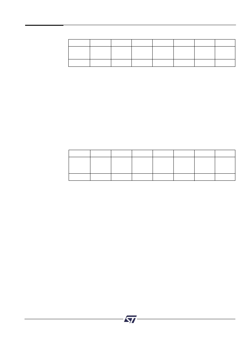
PSD835G2
PSD8XX Family
67
The
PSD835G2
Functional
Blocks
(cont.)
Bit 7
Bit 6
Bit 5
Bit 4
Bit 3
Bit 2
Bit 1
Bit 0
*
PLD
array
DBE
PLD
array
ALE
PLD
**
array
CNTL2
PLD
**
array
CNTL1
PLD
**
array
CNTL0
*
PLD
array
Addr.
1 = off
1 = off
1 = off
1 = off
1 = off
1 = off
PMMR2
Bit 0 0 = Address A[7:0] inputs to the PLD AND array are connected.
1 = Address A[7:0] inputs to the PLD AND array are disconnected, saving power.
Note:
In 80C51 mode, A[7:1] comes from Port F (PF1-PF3) and AD10 [3:0].
Bit 2 0 = Cntl0 input to the PLD AND array is connected.
1 = Cntl0 input to PLD AND array is disconnected, saving power.
Bit 3 0 = Cntl1 input to the PLD AND array is connected.
1 = Cntl1 input to PLD AND array is disconnected, saving power.
Bit 4 0 = Cntl2 input to the PLD AND array is connected.
1 = Cntl2 input to PLD AND array is disconnected, saving power.
Bit 5 0 = ALE input to the PLD AND array is connected.
1 = ALE input to PLD AND array is disconnected, saving power.
Bit 6 0 = DBE input to the PLD AND array is connected.
1 = DBE input to PLD AND array is disconnected, saving power.
*
*
Unused bits should be set to 0.
**
Refer to Table 14 the signals that are blocked on pins CNTL0-2.
Bit 1 0 = Automatic Power Down (APD) is disabled.
1 = Automatic Power Down (APD) is enabled.
Bit 3 0 = PLD Turbo is on.
1 = PLD Turbo is off, saving power.
Bit 4 0 = CLKIN input to the PLD AND array is connected.
Every CLKIN change will power up the PLD when Turbo bit is off.
1 = CLKIN input to PLD AND array is disconnected, saving power.
Bit 5 0 = CLKIN input to the PLD Micro
Cells is connected.
1 = CLKIN input to PLD Micro
Cells is disconnected, saving power.
Bit 7
Bit 6
Bit 5
Bit 4
Bit 3
Bit 2
Bit 1
Bit 0
*
*
PLD
Mcell clk
PLD
PLD
Turbo
*
APD
Enable
*
Array clk
1 = off
1 = off
1 = off
1 = on
Table 27. Power Management Mode Registers (PMMR0, PMMR2)**
PMMR0
**
*
Bits 0, 2, 6, and 7 are not used, and should be set to 0.
*
**
The PMMR0, and PMMR2 register bits are cleared to zero following power up.
***
Subsequent reset pulses will not clear the registers.
相关PDF资料 |
PDF描述 |
|---|---|
| PSD835G2V-A-20JI | Configurable Memory System on a Chip for 8-Bit Microcontrollers |
| PSD835G2V-A-20M | Configurable Memory System on a Chip for 8-Bit Microcontrollers |
| PSD835G2V-A-20MI | Configurable Memory System on a Chip for 8-Bit Microcontrollers |
| PSD835G2V-A-20U | Configurable Memory System on a Chip for 8-Bit Microcontrollers |
| PSD835G2V-A-20UI | Configurable Memory System on a Chip for 8-Bit Microcontrollers |
相关代理商/技术参数 |
参数描述 |
|---|---|
| PSD853F2-70J | 功能描述:SPLD - 简单可编程逻辑器件 5.0V 1M 70ns RoHS:否 制造商:Texas Instruments 逻辑系列:TICPAL22V10Z 大电池数量:10 最大工作频率:66 MHz 延迟时间:25 ns 工作电源电压:4.75 V to 5.25 V 电源电流:100 uA 最大工作温度:+ 75 C 最小工作温度:0 C 安装风格:Through Hole 封装 / 箱体:DIP-24 |
| PSD853F2-70M | 功能描述:CPLD - 复杂可编程逻辑器件 5.0V 1M 70ns RoHS:否 制造商:Lattice 系列: 存储类型:EEPROM 大电池数量:128 最大工作频率:333 MHz 延迟时间:2.7 ns 可编程输入/输出端数量:64 工作电源电压:3.3 V 最大工作温度:+ 90 C 最小工作温度:0 C 封装 / 箱体:TQFP-100 |
| PSD853F2-90J | 功能描述:CPLD - 复杂可编程逻辑器件 5.0V 1M 90ns RoHS:否 制造商:Lattice 系列: 存储类型:EEPROM 大电池数量:128 最大工作频率:333 MHz 延迟时间:2.7 ns 可编程输入/输出端数量:64 工作电源电压:3.3 V 最大工作温度:+ 90 C 最小工作温度:0 C 封装 / 箱体:TQFP-100 |
| PSD853F2-90JI | 功能描述:CPLD - 复杂可编程逻辑器件 5.0V 1M 90ns RoHS:否 制造商:Lattice 系列: 存储类型:EEPROM 大电池数量:128 最大工作频率:333 MHz 延迟时间:2.7 ns 可编程输入/输出端数量:64 工作电源电压:3.3 V 最大工作温度:+ 90 C 最小工作温度:0 C 封装 / 箱体:TQFP-100 |
| PSD853F2-90M | 功能描述:CPLD - 复杂可编程逻辑器件 5.0V 1M 90ns RoHS:否 制造商:Lattice 系列: 存储类型:EEPROM 大电池数量:128 最大工作频率:333 MHz 延迟时间:2.7 ns 可编程输入/输出端数量:64 工作电源电压:3.3 V 最大工作温度:+ 90 C 最小工作温度:0 C 封装 / 箱体:TQFP-100 |
发布紧急采购,3分钟左右您将得到回复。